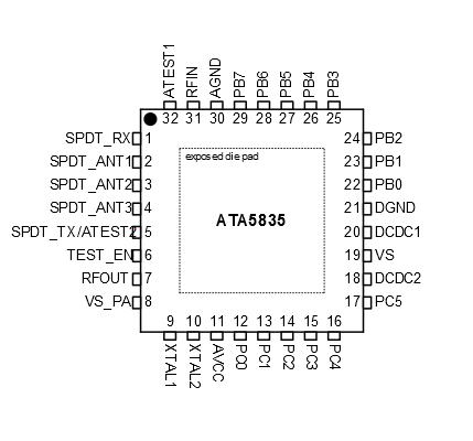
| Pin No. | Pin Name | Type | Equivalent Circuit | Description |
|---|---|---|---|---|
| 1 | SPDT_RX | Analog |  |
RF switch RX output |
| 2 | SPDT_ANT1 | Analog | RF switch antenna port 1 | |
| 3 | SPDT_ANT2 | Analog | RF switch antenna port 2 | |
| 4 | SPDT_ANT3 | Analog | RF switch antenna port 3 | |
| 5 | SPDT_TX/ATEST2 | Analog |  |
RF switch TX input RF front-end test I/O2 (only in Test mode) |
| 6 | TEST_EN | Analog | — | Connect Test enable to GND within the application. |
| 7 | RFOUT | Analog |  |
Power amplifier output |
| 8 | VS_PA | — | Power amplifier supply input (3V application) Power amplifier supply output (5V application) |
|
| 9 | XTAL1 | Analog |  |
Crystal oscillator input External clock input |
| 10 | XTAL2 | Analog | Crystal oscillator output | |
| 11 | AVCC | — | ESD protection circuit | RF front-end supply regulator output |
| 12 | PC0 | Digital |  |
Main: AVR® Digital I/O Port C0 Alternate: PCINT8/NRESET/DebugWIRE |
| 13 | PC1 | Digital | See pin PC0 | Main: AVR® Digital I/O Port C1 Alternate: NPWRON1/PCINT9/EXT_CLK |
| 14 | PC2 | Digital | See pin PC0 | Main: AVR® Digital I/O Port C2 Alternate: NPWRON2/PCINT10/TRPA |
| 15 | PC3 | Digital | See pin PC0 | Main: AVR® Digital I/O Port C3 Alternate: NPWRON3/PCINT11/TxD/TMDO |
| 16 | PC4 | Digital | See pin PC0 | Main: AVR® Digital I/O Port C4 Alternate: NPWRON4/PCINT12/RxD/INT0/TMDI |
| 17 | PC5 | Digital | See pin PC0 | Main: AVR® Digital I/O Port C5 Alternate: NPWRON5/PCINT13/TRPB/TMDO_CLK |
| 18 | DCDC2 | Analog |  |
DC-DC Converter pin 2 |
| 19 | VS | Analog | ESD protection circuit | Main supply voltage input |
| 20 | DCDC1 | Analog | See pin 18 (DCDC2) | DC-DC Converter pin 1 |
| 21 | DGND | — | ESD protection circuit | Digital ground |
| 22 | PB0 | Digital | See pin PC0 | Main: AVR® Digital I/O Port B0 Alternate: PCINT0/CLK_OUT |
| 23 | PB1 | Digital | See pin PC0 | Main: AVR® Digital I/O Port B1 Alternate: PCINT1/SCK |
| 24 | PB2 | Digital | See pin PC0 | Main: AVR® Digital I/O Port B2 Alternate: PCINT2/MOSI |
| 25 | PB3 | Digital | See pin PC0 | Main: AVR® Digital I/O Port B3 Alternate: PCINT3/MISO |
| 26 | PB4 | Digital | See pin PC0 | Main: AVR® Digital I/O Port B4 Alternate: PWRON/PCINT4/LED1 |
| 27 | PB5 | Digital | See pin PC0 | Main: AVR® Digital I/O Port B5 Alternate: PCINT5/INT1/NSS |
| 28 | PB6 | Digital | See pin PC0 | Main: AVR® Digital I/O Port B6 Alternate: PCINT6/EVENT |
| 29 | PB7 | Digital | See pin PC0 | Main: AVR® Digital I/O Port B7 Alternate: NPWRON6/PCINT7/RX_ACTIVE/LED0 |
| 30 | AGND | — | ESD protection circuit | Analog ground |
| 31 | RFIN | Analog |  |
LNA input |
| 32 | ATEST1 | Analog | — | RF front-end test I/O1, connected to GND in application |
| GND | — | — | Ground/backplane on exposed die pad |