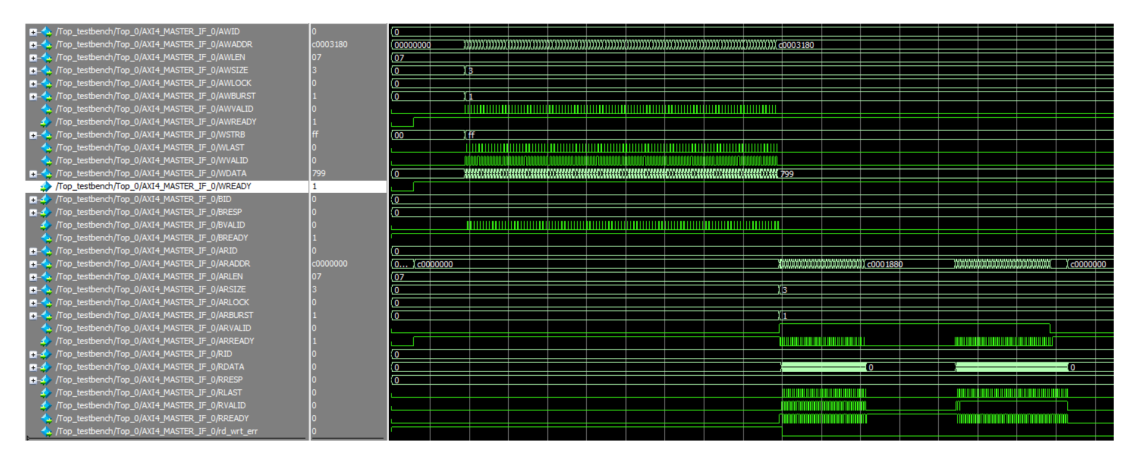
The following figure shows the simulation of write and read transactions to non-cached DDR region through FIC_0. FIC_0 operates at 250 MHz in this example.
Figure 1. Write and Read Transactions through FIC_0
The following figure shows the simulation of write and read transactions to non-cached DDR region through FIC_0. FIC_0 operates at 250 MHz in this example.