The dedicated UPDI pad is configured as an input with a pull-up.
When the pull-up is detected, the debugger initiates the enable sequence by driving the line low for a duration of tDeb0, as depicted in Figure 1:
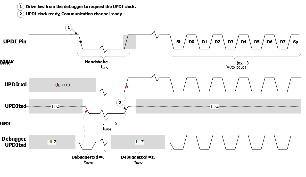
| Timing Label | Max. | Min. |
|---|---|---|
| tRES | 200 µs | 10 µs |
| tUPDI | 200 µs | 10 µs |
| tDeb0 | 1 µs | 200 ns |
| tDebZ | 14 ms | 200 µs |
When the negative edge is detected, the UPDI clock starts. The UPDI will continue to drive the line low until the clock is stable and ready for the UPDI to use. The duration of tUPDI will vary, depending on the status of the oscillator when the UPDI is enabled. After this duration, the data line will be released by the UPDI and pulled high.
When the debugger detects that the line is high, the initial SYNCH character
0x55 must be transmitted to synchronize the UPDI communication data
rate. If the Start bit of the SYNCH character is not sent within maximum
tDebZ, the UPDI will disable itself, and the UPDI enabling sequence must
be reinitiated. If the timing is violated, the UPDI is disabled to avoid unintentional
enabling of the UPDI.
After a successful SYNCH character transmission, the first instruction frame can be transmitted.