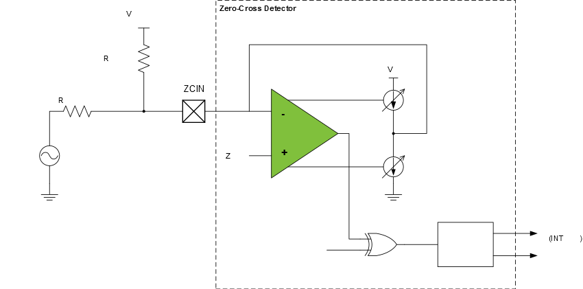
When the External Voltage source is referenced to ground
When the External Voltage source is referenced to VDD
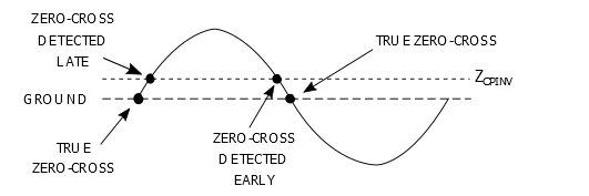
This offset time can be compensated by adding a pull-up or pull-down biasing resistor to the ZCD input pin. A pull-up resistor is used when the external voltage source is referenced to ground, as shown in the figure below.
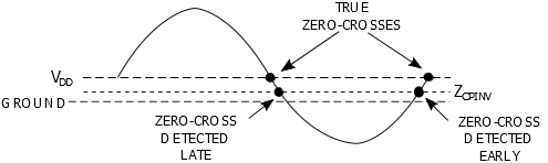
A pull-down resistor is used when the voltage is referenced to VDD, as shown in the figure below.
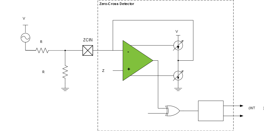
The resistor adds a bias to the ZCD input pin so that the external voltage source must go to zero to pull the pin voltage to the ZCPINV switching voltage. The pull-up or pull-down value can be determined with the equations shown below.
When the External Voltage source is referenced to ground
When the External Voltage source is referenced to VDD