For read/write operations, the Flash memory can be accessed either from the
code space or from the CPU data space. When the code space is used, the Flash is
accessible through the LPM and SPM instructions.
Additionally, the Flash memory is byte accessible when accessed through
the CPU data space. This means that it shares the same address space and instructions as
SRAM, EEPROM, and I/O registers and is accessible using LD/ST
instructions in assembly.
For the LPM and SPM instructions, address
0x0000 is the start of the Flash, but for LD and ST,
it is 0x8000, as shown in the Memory map section.
Addressing Flash Memory in Code Space
For read and write access to the Flash memory in the code space, the RAMPZ register is concatenated with the Z register to create the Address Pointer used for LPM/SPM access.
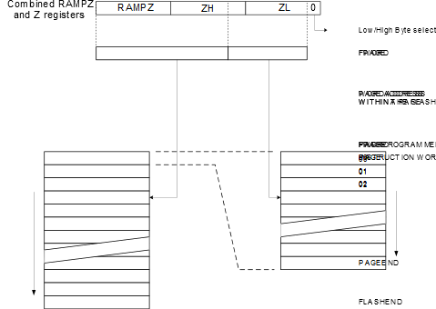
The Flash is word-accessed and organized in pages, so the Address Pointer can be treated as having two sections, as shown in Figure 1. The word address in the page (FWORD) is held by the Least Significant bits in the Address Pointer, while the Most Significant bits in the Address Pointer hold the Flash page address (FPAGE). Together, FWORD and FPAGE hold an absolute address to a word in the Flash.
The Flash is word-accessed for code space write operations, so the Least Significant bit (bit 0) in the Address Pointer is ignored.
For Flash read operations, one byte is read at a time. For this,
the Least Significant bit (bit 0) in the Address Pointer is used to select the low byte
or high byte in the word address. If this bit is ‘0’, the low byte is
read, and if this bit is ‘1’, the high byte is read.
Once a programming operation is initiated, the address is latched, and the Address Pointer can be updated and used for other operations.
Addressing Flash in CPU Data Space
The Flash area in data space has only 32 KB. For devices with Flash memory size greater than 32 KB, the Flash memory is divided into blocks of 32 KB. Those blocks are mapped into data space using the FLMAP bit field of the NVMCTRL.CTRLB register.
For read and write access to the Flash memory in the CPU data space, the
LD/ST instructions are used to access one byte at a
time.