Independent of the setting of Data Direction bit DDxn, the port pin can be read through the PINxn Register bit. As shown in Figure 1, the PINxn Register bit and the preceding latch constitute a synchronizer. This is needed to avoid metastability if the physical pin changes value near the edge of the internal clock, but it also introduces a delay. The following figure shows a timing diagram of the synchronization when reading an externally applied pin value. The maximum and minimum propagation delays are denoted tpd,max and tpd,min respectively.
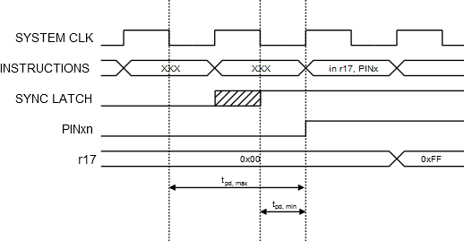
Consider the clock period starting shortly after the first falling edge of the system clock. The latch is closed when the clock is low, and goes transparent when the clock is high, as indicated by the shaded region of the “SYNC LATCH” signal. The signal value is latched when the system clock goes low. It is clocked into the PINxn Register at the succeeding positive clock edge. As indicated by the two arrows tpd,max and tpd,min, a single signal transition on the pin will be delayed between ½ and 1½ system clock period depending upon the time of assertion.
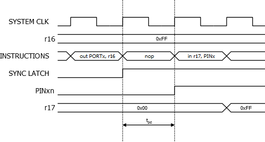
When reading back a software assigned pin value, a nop instruction must be inserted as indicated in the following figure. The out instruction sets the “SYNC LATCH” signal at the positive edge of the clock. In this case, the delay tpd through the synchronizer is 1 system clock period.