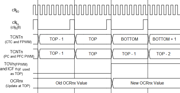
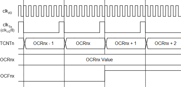
The Timer/Counter is a synchronous design and the timer clock (clkT0) is therefore shown as a clock enable signal in the following figures. The figures include information on when Interrupt Flags are set, and when the OCR0x Register is updated with the OCR0x buffer value (only for modes utilizing double buffering). The first figure shows a timing diagram for the setting of OCF0x.
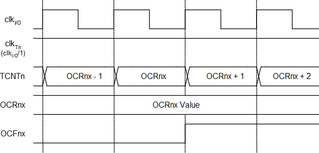
The next figure shows the same timing data, but with the prescaler enabled.
The next figure shows the count sequence close to TOP in various modes. When using phase and frequency correct PWM mode the OCR0x Register is updated at BOTTOM. The timing diagrams will be the same, but TOP should be replaced by BOTTOM, TOP-1 by BOTTOM+1 and so on. The same renaming applies for modes that set the TOV0 Flag at BOTTOM.
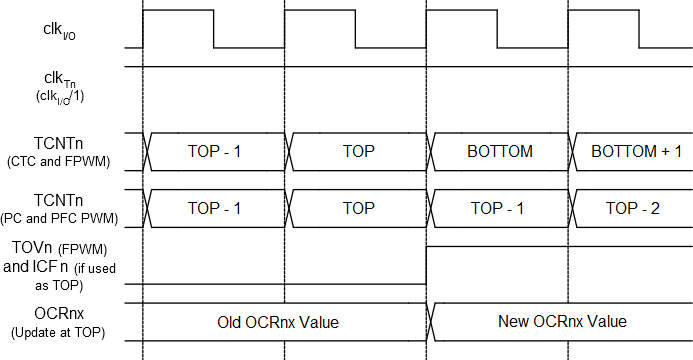
The next figure shows the same timing data, but with the prescaler enabled.