The Fast Pulse Width Modulation or Fast PWM modes (modes 5, 6, 7, 14,and 15, WGM0[3:0]= 0x5, 0x6, 0x7, 0xE, 0xF) provide a high frequency PWM waveform generation option. The Fast PWM differs from the other PWM options by its single-slope operation. The counter counts from BOTTOM to TOP then restarts from BOTTOM.
In non-inverting Compare Output mode, the Output Compare (OC0x) is cleared on the compare match between TCNT0 and OCR0x, and set at BOTTOM. In inverting Compare Output mode output is set on compare match and cleared at BOTTOM. Due to the single-slope operation, the operating frequency of the Fast PWM mode can be twice as high as the phase correct and phase and frequency correct PWM modes that use dual-slope operation. This high frequency makes the Fast PWM mode well suited for power regulation, rectification, and DAC applications. High frequency allows physically small sized external components (coils, capacitors), hence reduces total system cost.
The PWM resolution for Fast PWM can be fixed to 8-, 9-, or 10-bit, or defined by either ICR0 or OCR0A. The minimum resolution allowed is 2-bit (ICR0 or OCR0A register set to 0x0003), and the maximum resolution is 16-bit (ICR0 or OCR0A registers set to MAX). The PWM resolution in bits can be calculated by using the following equation:
In Fast PWM mode the counter is incremented until the counter value matches either one of the fixed values 0x00FF, 0x01FF, or 0x03FF (WGM0[3:0] = 0x5, 0x6, or 0x7), the value in ICR0 (WGM0[3:0]=0xE), or the value in OCR0A (WGM0[3:0]=0xF). The counter is then cleared at the following timer clock cycle. The timing diagram for the Fast PWM mode using OCR0A or ICR0 to define TOP is shown below. The TCNT0 value is in the timing diagram shown as a histogram for illustrating the single-slope operation. The diagram includes non-inverted and inverted PWM outputs. The small horizontal lines on the TCNT0 slopes mark compare matches between OCR0x and TCNT0. The OC0x Interrupt Flag will be set when a compare match occurs.
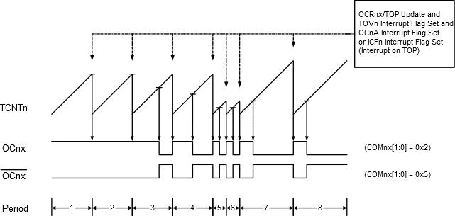
The Timer/Counter Overflow Flag (TOV0) is set each time the counter reaches TOP. In addition, when either OCR0A or ICR0 is used for defining the TOP value, the OC0A or ICF0 Flag is set at the same timer clock cycle TOV0 is set. If one of the interrupts are enabled, the interrupt handler routine can be used for updating the TOP and compare values.
When changing the TOP value the program must ensure that the new TOP value is higher or equal to the value of all of the Compare Registers. If the TOP value is lower than any of the Compare Registers, a compare match will never occur between the TCNT0 and the OCR0x. Note that when using fixed TOP values the unused bits are masked to zero when any of the OCR0x Registers are written.
The procedure for updating ICR0 differs from updating OCR0A when used for defining the TOP value. The ICR0 Register is not double buffered. This means that if ICR0 is changed to a low value when the counter is running with none or a low prescaler value, there is a risk that the new ICR0 value written is lower than the current value of TCNT0. As result, the counter will miss the compare match at the TOP value. The counter will then have to count to the MAX value (0xFFFF) and wrap around starting at 0x0000 before the compare match can occur. The OCR0A Register however, is double buffered. This feature allows the OCR0A I/O location to be written anytime. When the OCR0A I/O location is written the value written will be put into the OCR0A Buffer Register. The OCR0A Compare Register will then be updated with the value in the Buffer Register at the next timer clock cycle the TCNT0 matches TOP. The update is done at the same timer clock cycle as the TCNT0 is cleared and the TOV0 Flag is set.
Using the ICR0 Register for defining TOP works well when using fixed TOP values. By using ICR0, the OCR0A Register is free to be used for generating a PWM output on OC0A. However, if the base PWM frequency is actively changed (by changing the TOP value), using the OCR0A as TOP is clearly a better choice due to its double buffer feature.
In Fast PWM mode, the compare units allow generation of PWM waveforms on the OC0x pins. Writing the COM0x[1:0] bits to 0x2 will produce an inverted PWM and a non-inverted PWM output can be generated by writing the COM0x[1:0] to 0x3. The actual OC0x value will only be visible on the port pin if the data direction for the port pin is set as output (DDR_OC0x). The PWM waveform is generated by setting (or clearing) the OC0x Register at the compare match between OCR0x and TCNT0, and clearing (or setting) the OC0x Register at the timer clock cycle the counter is cleared (changes from TOP to BOTTOM).
The PWM frequency for the output can be calculated by the following equation:
- The “n” in the register and bit names indicates the device number (n = 0 for Timer/Counter 0), and the “x” indicates Output Compare unit (A/B).
- N represents the prescale divider (1, 8, 64, 256, or 1024).
The extreme values for the OCR0x registers represents special cases when generating a PWM waveform output in the Fast PWM mode. If the OCR0x is set equal to BOTTOM (0x0000) the output will be a narrow spike for each TOP+1 timer clock cycle. Setting the OCR0x equal to TOP will result in a constant high or low output (depending on the polarity of the output which is controlled by COM0x[1:0]).
A frequency waveform output with 50% duty cycle can be achieved in Fast PWM mode by selecting OC0A to toggle its logical level on each compare match (COM0A[1:0]=0x1). This applies only if OCR0A is used to define the TOP value (WGM0[3:0]=0xF). The waveform generated will have a maximum frequency of fOC0A = fclk_I/O/2 when OCR0A is set to zero (0x0000). This feature is similar to the OC0A toggle in CTC mode, except the double buffer feature of the Output Compare unit is enabled in the Fast PWM mode.