The phase and frequency correct Pulse Width Modulation, or phase and frequency correct PWM mode (WGM0[3:0] = 0x8 or 0x9) provides a high resolution phase and frequency correct PWM waveform generation option. The phase and frequency correct PWM mode is, like the phase correct PWM mode, based on a dual-slope operation. The counter counts repeatedly from BOTTOM (0x0000) to TOP and then from TOP to BOTTOM. In non-inverting Compare Output mode, the Output Compare (OC0x) is cleared on the compare match between TCNT0 and OCR0x while up-counting, and set on the compare match while down-counting. In inverting Compare Output mode, the operation is inverted. The dual-slope operation gives a lower maximum operation frequency compared to the single-slope operation. However, due to the symmetric feature of the dual-slope PWM modes, these modes are preferred for motor control applications.
The main difference between the phase correct, and the phase and frequency correct PWM mode is the time the OCR0x Register is updated by the OCR0x Buffer Register, (see Figure 1 and the Timing Diagram below).
The PWM resolution for the phase and frequency correct PWM mode can be defined by either ICR0 or OCR0A. The minimum resolution allowed is 2-bit (ICR0 or OCR0A set to 0x0003), and the maximum resolution is 16-bit (ICR0 or OCR0A set to MAX). The PWM resolution in bits can be calculated using the following equation:
In phase and frequency correct PWM mode the counter is incremented until the counter value matches either the value in ICR0 (WGM0[3:0]=0x8), or the value in OCR0A (WGM0[3:0]=0x9). The counter has then reached the TOP and changes the count direction. The TCNT0 value will be equal to TOP for one timer clock cycle. The timing diagram for the phase correct and frequency correct PWM mode is shown below. The figure shows phase and frequency correct PWM mode when OCR0A or ICR0 is used to define TOP. The TCNT0 value is in the timing diagram shown as a histogram for illustrating the dual-slope operation. The diagram includes non-inverted and inverted PWM outputs. The small horizontal line marks on the TCNT0 slopes represent compare matches between OCR0x and TCNT0. The OC0x Interrupt Flag will be set when a compare match occurs.
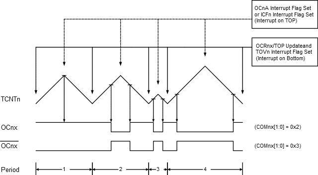
The Timer/Counter Overflow Flag (TOV0) is set at the same timer clock cycle as the OCR0x Registers are updated with the double buffer value (at BOTTOM). When either OCR0A or ICR0 is used for defining the TOP value, the OC0A or ICF0 Flag set when TCNT0 has reached TOP. The Interrupt Flags can then be used to generate an interrupt each time the counter reaches the TOP or BOTTOM value.
When changing the TOP value the program must ensure that the new TOP value is higher or equal to the value of all of the Compare Registers. If the TOP value is lower than any of the Compare Registers, a compare match will never occur between the TCNT0 and the OCR0x.
As shown in the timing diagram above, the output generated is, in contrast to the phase correct mode, symmetrical in all periods. Since the OCR0x Registers are updated at BOTTOM, the length of the rising and the falling slopes will always be equal. This gives symmetrical output pulses and is therefore frequency correct.
Using the ICR0 Register for defining TOP works well when using fixed TOP values. By using ICR0, the OCR0A Register is free to be used for generating a PWM output on OC0A. However, if the base PWM frequency is actively changed by changing the TOP value, using the OCR0A as TOP is clearly a better choice due to its double buffer feature.
In phase and frequency correct PWM mode, the compare units allow generation of PWM waveforms on the OC0x pins. Setting the COM0x[1:0] bits to 0x2 will produce a non-inverted PWM and an inverted PWM output can be generated by setting the COM0x[1:0] to 0x3 (See description of TCCRA.COM0x). The actual OC0x value will only be visible on the port pin if the data direction for the port pin is set as output (DDR_OC0x). The PWM waveform is generated by setting (or clearing) the OC0x Register at the compare match between OCR0x and TCNT0 when the counter increments, and clearing (or setting) the OC0x Register at compare match between OCR0x and TCNT0 when the counter decrements. The PWM frequency for the output when using phase and frequency correct PWM can be calculated by the following equation:
- The “n” in the register and bit names indicates the device number (n = 0 for Timer/Counter 0), and the “x” indicates Output Compare unit (A/B).
- N represents the prescale divider (1, 8, 64, 256, or 1024).
The extreme values for the OCR0x Register represents special cases when generating a PWM waveform output in the phase correct PWM mode. If the OCR0x is set equal to BOTTOM the output will be continuously low and if set equal to TOP the output will be set to high for non-inverted PWM mode. For inverted PWM the output will have the opposite logic values. If OCR0A is used to define the TOP value (WGM0[3:0]=0x9) and COM0A[1:0]=0x1, the OC0A output will toggle with a 50% duty cycle.