The following characteristics are applicable to the operating temperature range: TA [-40°C : +105°C], unless otherwise specified.
| Symbol | Parameter | Conditions | Min. | Typ. | Max. | Unit |
|---|---|---|---|---|---|---|
| VDDCORE | DC Supply Core | – | 1.20 | – | 1.32 | V |
| Allowable Voltage Ripple | rms value 10 kHz to 20 MHz | – | – | 20 | mV | |
| Rising Slope (2) | – | 1.20 | – | 30 | V/ms | |
| VDDIO | DC Supply I/Os, Backup | (See Note 1) | 3.0 | 3.3 | 3.6 | V |
| Allowable Voltage Ripple | rms value 10 kHz to 10 MHz | – | – | 30 | mV | |
| Rising Slope | – | 6.5 | – | 30 | V/ms | |
| VDDIN | DC Supply Voltage Regulator | (See Note 1) | 3.0 | 3.3 | 3.6 | V |
| Allowable Voltage Ripple | rms value 10 kHz to 20 MHz | – | – | 20 | mv | |
| VDDPLL | PLL A and Main Oscillator Supply | – | 1.20 | – | 1.32 | V |
| Allowable Voltage Ripple | rms value 10 kHz to 10 MHz | – | – | 20 | mV | |
| rms value > 10 MHz | – | – | 10 | |||
| VDDUTMIC | DC Supply UDPHS and UHPHS UTMI+ Core | – | 1.20 | – | 1.32 | V |
| Allowable Voltage Ripple | rms value 10 kHz to 10 MHz | – | – | 10 | mV | |
| VDDUTMII | DC Supply UDPHS and UHPHS UTMI+ Interface | – | 3.0 | 3.3 | 3.6 | V |
| Allowable Voltage Ripple | rms value 10 kHz to 10 MHz | – | – | 20 | mV | |
| VDDPLLUSB | DC Supply UTMI PLL | – | 3.0 | 3.3 | 3.6 | V |
| Allowable Voltage Ripple | rms value 10 kHz to 10 MHz | – | – | 10 | mV |
Notes:
- 1.VDDIO voltage must be equal to VDDIN voltage.
- 2.Refer to section 7.2.1 Powerup.
| Symbol | Parameter | Conditions | Min. | Typ. | Max. | Unit |
|---|---|---|---|---|---|---|
| VIL | Low-level Input Voltage | GPIO_MLB | -0.3 | – | 0.7 | V |
| GPIO_AD, GPIO_CLK | -0.3 | – | 0.8 | |||
| GPIO, CLOCK, RST, TEST | -0.3 | – | VDDIO x 0.3 | |||
| VIH | High-level Input Voltage | GPIO_MLB | 1.80 | – | VDDIO + 0.3 | V |
| GPIO_AD, GPIO_CLK | 2 | VDDIO + 0.3 | ||||
| GPIO, CLOCK, RST, TEST | VDDIO x 0.7 | – | VDDIO + 0.3 | |||
| VOH | High-level Output Voltage | GPIO_MLB, IOH = 6 mA | 2 | – | – | V |
| GPIO_AD, GPIO, RST, TEST, CLOCK , IOH = 4 mA, Low drive | VDDIO - 0.4 | – | – | |||
| GPIO_AD, GPIO, RST, TEST, CLOCK , IOH = 10 mA,High drive | VDDIO - 0.4 | – | – | |||
| GPIO_CLK, IOH = 6 mA, Low drive | VDDIO - 0.4 | |||||
| GPIO_CLK,IOH = 12 mA, High drive | VDDIO - 0.4 | – | – | |||
| VOL | Low-level Output Voltage | GPIO_MLB, IOL = -6 mA | – | – | 0.4 | V |
| GPIO_AD, GPIO, RST, TEST, CLOCK, IOL = -4 mA, Low drive | – | – | 0.4 | |||
| GPIO_AD, GPIO, RST, TEST, CLOCK, IOL = -10 mA,High drive | – | – | 0.4 | |||
| GPIO_CLK, IOL = -6 mA, Low drive | – | – | 0.4 | |||
| GPIO_CLK, IOL = -12 mA, High drive | – | – | 0.4 | |||
| Vhys | Hysteresis Voltage | GPIO with Hysteresis mode enabled | 150 | – | – | mV |
| IIL | Low-level Input Current | Pullup OFF | -1 | – | 1 | µA |
| Pullup ON | 10 | – | 55 | |||
| IIH | High-level Input Current | Pulldown OFF | -1 | – | 1 | µA |
| Pulldown ON | 10 | – | 55 | |||
| RSERIAL | Serial Resistor | GPIO_MLB | – | 9 | – | Ohm |
| GPIO_AD, GPIO_CLK | – | 14 | – | |||
| GPIO, CLOCK, RST, TEST | – | 26 | – |
| Symbol | Parameter | Conditions | Min. | Typ. | Max. | Unit |
|---|---|---|---|---|---|---|
| VDDOUT | DC Output Voltage | Normal mode, ILOAD = 100 mA | 1.2 | 1.23 | 1.26 | V |
| Standby mode | – | 0 | – | |||
| ILOAD | Maximum DC Output Current | – | – | 150 | mA | |
| CDIN | Input Decoupling Capacitor | (1) | – | 4.7 | – | µF |
| CDOUT | Output Decoupling Capacitor | (2) | – | 1 | – | µF |
| ESR | – | – | 2 | Ohm | ||
| tON | Turn-on Time | CDOUT = 1 µF, VDDOUT reaches DC output voltage | – | 1 | 2.5 | ms |
Notes:
- 1.A 4.7 μF (±20%) or higher ceramic capacitor must be connected between VDDIN and the closest GND pin of the device. This large decoupling capacitor is mandatory to reduce startup current, improving transient response and noise rejection.
- 2.To ensure stability, an external 1 μF (±20%) output capacitor, CDOUT, must be connected between VDDOUT and the closest GND pin of the device. Solid tantalum and multilayer ceramic capacitors are suitable as output capacitors. A 100 nF bypass capacitor between VDDOUT and the closest GND pin of the device helps decrease output noise and improves the load transient response.
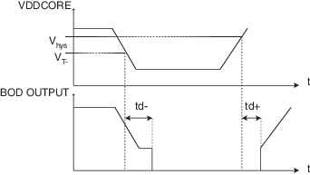
| Symbol | Parameter | Conditions | Min. | Typ. | Max. | Unit |
|---|---|---|---|---|---|---|
| VT- | Supply Falling Threshold (see Note 1) | – | 0.97 | 1.0 | 1.04 | V |
| Vhys | Hysteresis Voltage | – | – | 25 | 50 | mV |
| tSTART | Startup Time | From disabled state to enabled state | – | – | 400 | µs |
Note:
- 1.The Brownout Detector is configured using the BODDIS bit in the SUPC_MR register.
Figure 1. Core Brownout Output Waveform
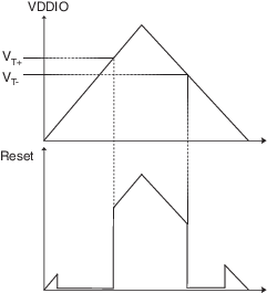
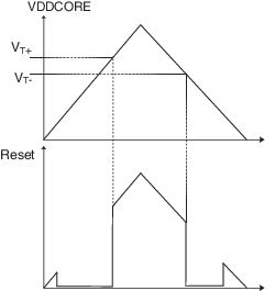
| Symbol | Parameter | Conditions | Min. | Typ. | Max. | Unit |
|---|---|---|---|---|---|---|
| VT+ | Threshold Voltage Rising | – | 0.79 | 0.95 | 1.07 | V |
| VT- | Threshold Voltage Falling | – | 0.66 | 0.89 | – | V |
| Vhys | Hysteresis Voltage | – | 10 | 60 | 115 | mV |
| tRES | Reset Timeout Period | – | 240 | 350 | 800 | µs |
Figure 2. VDDCORE Power-On Reset Characteristics
| Symbol | Parameter | Conditions | Min. | Typ. | Max. | Unit |
|---|---|---|---|---|---|---|
| VT | Supply Monitor Threshold | 16 selectable steps (see the Threshold Selection table below) | – | – | – | V |
| TACC | Threshold Accuracy | – | -4 | – | 4 | % |
| Vhys | Hysteresis Voltage | – | – | 38 | 45 | mV |
| tSTART | Startup Time | From disabled state to enabled state | – | – | 300 | µs |
Notes:
- 1.It is recommended to enable the Supply Monitor (see Table 58-9 Threshold selection).
- 2.The Supply Monitor operates down to 1.7V.
- 3.Once the Supply Monitor threshold is reached, it takes <200 µs to generate the internal reset of the device. The internal reset will remain active all the way until the POR becomes active.
- 4.The 200 us reset time parameter is for design guidance only, and is not tested in manufacturing.
| Symbol | Parameter | Digital Code | Min. | Typ. | Max. | Unit |
|---|---|---|---|---|---|---|
| VT | Supply Monitor Threshold | 0 | – | 1.6 | – | V |
| 1 | – | 1.72 | – | |||
| 10 | – | 1.84 | – | |||
| 11 | – | 1.96 | – | |||
| 100 | – | 2.08 | – | |||
| 101 | – | 2.2 | – | |||
| 110 | – | 2.32 | – | |||
| 111 | – | 2.44 | – | |||
| 1000 | – | 2.56 | – | |||
| 1001 | – | 2.68 | – | |||
| 1010 | – | 2.8 | – | |||
| 1011 | – | 2.92 | – | |||
| 1100 | – | 3.04 | – | |||
| 1101 | – | 3.16 | – | |||
| 1110 | – | 3.28 | – | |||
| 1111 | – | 3.4 | – |
Figure 3. VDDIO Supply Monitor

| Symbol | Parameter | Conditions | Min. | Typ. | Max. | Unit |
|---|---|---|---|---|---|---|
| VT+ | Threshold Voltage Rising | – | 1.45 | 1.53 | 1.61 | V |
| VT- | Threshold Voltage Falling | – | 1.37 | 1.46 | – | V |
| Vhys | Hysteresis | – | 40 | 80 | 130 | mV |
| tRES | Reset Time-out Period | – | 240 | 320 | 800 | µs |
Figure 4. VDDIO Power-On Reset Characteristics