| Signal Name | Recommended Pin Connection | Description | |
|---|---|---|---|
| SWCLK/TCK | Pullup (100 kOhm)(1)
If debug mode is not required, this pin can be used as GPIO. |
Serial Wire Clock / Test Clock (Boundary scan mode only) This pin is a Schmitt trigger input. No internal pullup resistor at reset. |
|
| SWDIO/TMS | Pullup (100 kOhm) (1) If debug mode is not required, this pin can be used as GPIO. |
Serial Wire Input-Output / Test Mode Select (Boundary scan mode only). This pin is a Schmitt trigger input. No internal pullup resistor at reset. |
|
| TDI | Floating. If boundary mode is not required, this pin can be used as GPIO. |
Test Data In (Boundary scan mode only) This pin is a Schmitt trigger input. No internal pullup resistor at reset. |
|
| TRACESWO/TDO | Floating. If boundary mode is not required, this pin can be used as GPIO. |
Test Data Out (Boundary scan mode only) Output driven at up to VDDIO |
|
| JTAGSEL | In harsh environments(2), it is strongly recommended to tie this pin to GND if not used or to add an external low-value resistor (such as 1 kOhm). | JTAG Selection. Internal permanent pulldown resistor to GNDBU (15 kOhm). Must be tied to VDDIO to enter JTAG Boundary Scan with TST tied to VDDIO and PD0 tied to GND. |
Figure 1. SWD Schematic Example with a 10-pin Connector
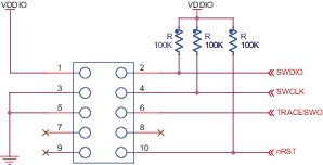
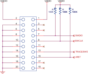
Figure 2. SWD Schematic Example with a 20-pin Connector
Notes:
- 1.These values are given only as a typical example.
- 2.In a well-shielded environment subject to low magnetic and electric field interference, the pin may be left unconnected. In noisy environments, a connection to ground is recommended.