Both preview and codec datapaths contain FIFOs. These asynchronous buffers are used to safely transfer formatted pixels from the pixel clock domain to the AHB clock domain. A video arbiter is used to manage FIFO thresholds and triggers a relevant DMA request through the AHB master interface. Thus, depending on the FIFO state, a specified length burst is asserted. Regarding AHB master interface, it supports Scatter DMA mode through linked list operation. This mode of operation improves flexibility of image buffer location and allows the user to allocate two or more frame buffers. The destination frame buffers are defined by a series of Frame Buffer Descriptors (FBD). Each FBD controls the transfer of one entire frame and then optionally loads a further FBD to switch the DMA operation at another frame buffer address. The FBD is defined by a series of three words. The first word defines the current frame buffer address (named DMA_X_ADDR register), the second defines control information (named DMA_X_CTRL register) and the third defines the next descriptor address (named DMA_X_DSCR). DMA Transfer mode with linked list support is available for both codec and preview datapaths. The data to be transferred described by an FBD requires several burst accesses. In the following example, the use of two ping-pong frame buffers is described.
Example:
The first FBD, stored at address 0x00030000, defines the location of the first frame buffer. This address is programmed in the ISI user interface DMA_P_DSCR. To enable the descriptor fetch operation, the value 0x00000001 must be written to the DMA_P_CTRL register. LLI_0 and LLI_1 are the two descriptors of the linked list.
Destination address: frame buffer ID0 0x02A000 (LLI_0.DMA_P_ADDR)
Transfer 0 Control Information, fetch and writeback: 0x00000003 (LLI_0.DMA_P_CTRL)
Next FBD address: 0x00030010 (LLI_0.DMA_P_DSCR)
The second FBD, stored at address 0x00030010, defines the location of the second frame buffer.
Destination address: frame buffer ID1 0x0003A000 (LLI_1.DMA_P_ADDR)
Transfer 1 Control information fetch and writeback: 0x00000003 (LLI_1.DMA_P_CTRL)
The third FBD address: 0x00030000, wrapping to first FBD (LLI_1.DMA_P_DSCR)
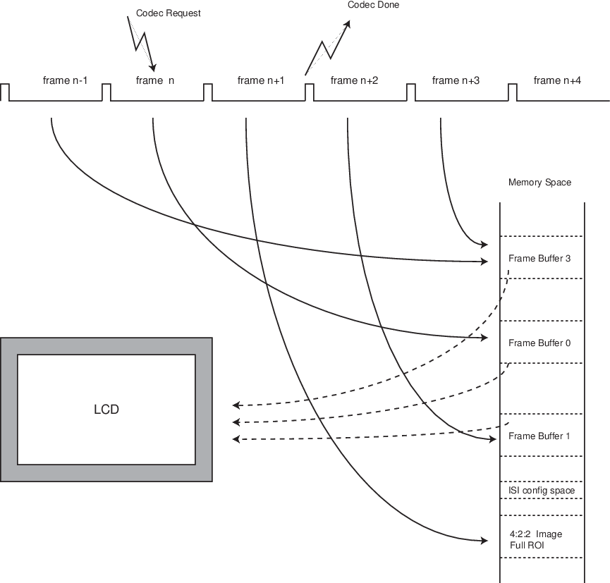
Using this technique, several frame buffers can be configured through the linked list. The following figure illustrates a typical three-frame buffer application. Frame n is mapped to frame buffer 0, frame n+1 is mapped to frame buffer 1, frame n+2 is mapped to frame buffer 2 and further frames wrap. A codec request occurs, and the full-size 4:2:2 encoded frame is stored in a dedicated memory space.