| Power Supplies Schematic Example with Internal Regulator Use | |||
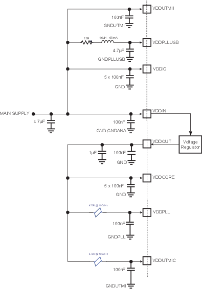 Note: Component values are given only as a typical example. Note: Restrictions With main supply < 2.5V, USB and DACC are not usable. With main supply > 2.5V and < 3V, USB is not usable. With main supply > 3.0 V, all peripherals are usable. |
| Check | Signal Name | Recommended Pin Connection | Description |
|---|---|---|---|
| VDDIN | Decoupling/filtering capacitors (100 nF and 4.7 μF)(1)(2) |
Powers the voltage regulator, AFE, DAC,
and Analog comparator power supply Supply ripple must not exceed 20 mVrms for 10 kHz to 20 MHz range. Warning: VDDIN and VDDIO must have the
same level and must be higher than VDDCORE.
Warning: Powerup and powerdown sequences given in the “Power Considerations” chapter must be
respected.
|
|
| VDDIO | Decoupling/filtering capacitors (100 nF)(1)(2) |
Powers the Peripheral I/O lines
(Input/Output Buffers), backup part, 1 Kbyte of Backup SRAM, 32 kHz crystal
oscillator, oscillator pads Decoupling/filtering capacitors must be added to improve startup stability and reduce source voltage drop. Supply ripple must not exceed 30 mVrms for 10 kHz to 10 MHz range. Warning: VDDIN and VDDIO
must have the same level and must be higher than VDDCORE.
Warning: Powerup and powerdown sequences given in the “Power Considerations” chapter must be
respected.
|
|
| VDDUTMII | Decoupling capacitor (100 nF)(1)(2) | Powers the USB transceiver interface.
Must be connected to VDDIO. For USB operations, VDDUTMII and VDDIO voltage ranges must be from 3.0V to 3.6V. Must always be connected even when the USB is not used. Decoupling/filtering capacitors must be added to improve startup stability and reduce source voltage drop. Supply ripple must not exceed 20 mVrms for 10 kHz to 10 MHz range. |
|
| VDDPLLUSB | Decoupling/filtering RLC circuit(1) | Powers the UTMI PLL and the 3 to 20 MHz
oscillator. The VDDPLLUSB power supply pin draws small current, but it is noise sensitive. Care must be taken in VDDPLLUSB power supply routing, decoupling and also on bypass capacitors. Supply ripple must not exceed 10 mVrms for 10 kHz to 10 MHz range. |
|
| VDDOUT | Decoupling capacitor (100 nF + 1 μF)(1)(2) |
Voltage Regulator Output | |
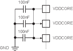
| VDDCORE | Decoupling capacitor (100 nF)(1)(2) | Powers the core, embedded memories and
peripherals. Decoupling/filtering capacitors must be added to improve startup stability and reduce source voltage drop. Warning: Powerup and powerdown sequences given in the
“Power Considerations” chapter must be
respected.
|
|
| VDDPLL | Decoupling/filtering capacitors ferrite
beads (100 nF and 470 Ohm @ 100MHz)(1)(2) |
Powers the PLLA and the fast RC
oscillator. The VDDPLL power supply pin draws small current, but it is noise sensitive. Care must be taken in VDDPLL power supply routing, decoupling and also on bypass capacitors. |
|
| VDDUTMIC | Decoupling/filtering capacitors ferrite
beads (100 nF and 470 Ohm @ 100MHz)(1)(2) |
Powers the USB transceiver core. Must always be connected even if the USB is not used. Decoupling/filtering capacitors/ferrite beads must be added to improve startup stability and reduce source voltage drop. |
|
| GND | Voltage Regulator, Core Chip and Peripheral I/O lines ground | GND pins are common to VDDIN, VDDCORE
and VDDIO pins. GND pins should be connected as shortly as possible to the system ground plane. |
|
| GNDUTMI | UDPHS and UHPHS UTMI+ Core and interface ground | GNDUTMI pins are common to VDDUTMII and
VDDUTMIC pins. GNDUTMI pins should be connected as shortly as possible to the system ground plane. |
|
| GNDPLL | PLLA cell and Main Oscillator ground | GNDPLL pin is provided for VDDPLL pin. GNDPLL pin should be connected as shortly as possible to the system ground plane. | |
| GNDANA | Analog ground | GNDANA pins are common to AFE, DAC and
ACC supplied by VDDIN pin. GNDANA pins should be connected as shortly as possible to the system ground plane. |
|
| GNDPLLUSB | USB PLL ground | The GNDPLLUSB pin is provided for VDDPLLUSB pin. The GNDPLLUSB pin should be connected as shortly as possible to the system ground plane. |
- 1.These values are given only as a typical example.
- 2.Decoupling capacitors must be connected as close as possible to the microcontroller and on each concerned pin, vias should be avoided.