| Name | Definition |
|---|---|
| TIMER_CLOCK1 | PCK6 or PCK7 (TC0 only) |
| TIMER_CLOCK2 | MCK/8 |
| TIMER_CLOCK3 | MCK/32 |
| TIMER_CLOCK4 | MCK/128 |
| TIMER_CLOCK5 (1) | SLCK |
- 1.When SLCK is selected for Peripheral Clock (CSS = 0 in PMC Master Clock register), SLCK input is equivalent to Peripheral Clock.
- 2.The PCK6 or PCK7 (TC0 only) frequency must be at least three times lower than peripheral clock frequency.
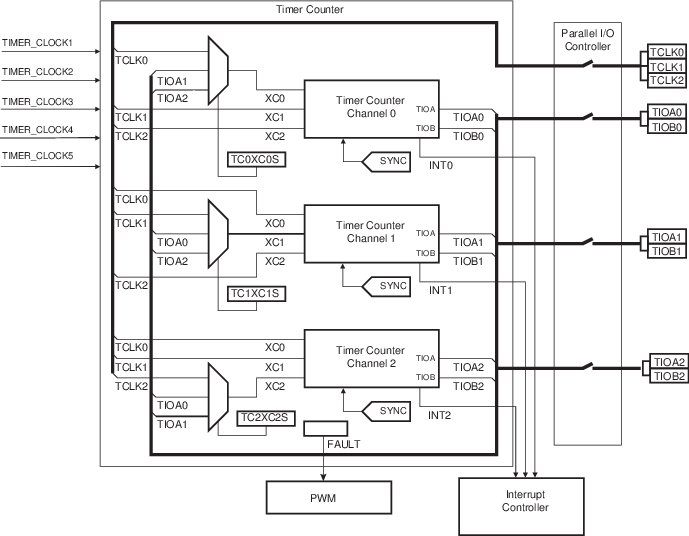
Figure 1. Timer Counter Block Diagram
Note:
The QDEC connections are detailed in Predefined Connection of the Quadrature Decoder with Timer Counters.
| Signal Name | Description |
|---|---|
| XC0, XC1, XC2 | External Clock Inputs |
| TIOAx | Capture Mode: Timer Counter Input Waveform Mode: Timer Counter Output |
| TIOBx | Capture Mode: Timer Counter Input Waveform Mode: Timer Counter Input/Output |
| INT | Interrupt Signal Output (internal signal) |
| SYNC | Synchronization Input Signal (from configuration register) |