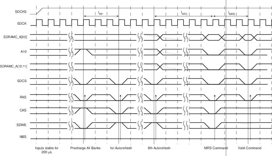
The initialization sequence is generated by software. The sequence to initialize SDRAM devices is the following:
- 1.Set the SDRAM features in the SDRAMC_CR: asynchronous timings (TRC, TRAS, etc.), number of columns, number of rows, CAS latency and data bus width. Set UNAL bit in SDRAMC_CFR1.
- 2.For mobile SDRAM, configure temperature-compensated self-refresh (TCSR), drive strength (DS) and partial array self-refresh (PASR) in the Low Power register (SDRAMC_LPR).
- 3.Select the SDRAM memory device type in the Memory Device register (SDRAMC_MDR).
- 4.A pause of at least 200 μs must be observed before a signal toggle.
- 5.A NOP command is issued to the SDRAM devices. The application must write a 1 to the MODE field in the Mode register (SDRAMC_MR) (see Note). Read the SDRAMC_MR and add a memory barrier assembler instruction just after the read. Perform a write access to any SDRAM address.
- 6.An All Banks Precharge command is issued to the SDRAM. The application must write a 2 to the MODE field in the SDRAMC_MR. Read the SDRAMC_MR and add a memory barrier assembler instruction just after the read. Perform a write access to any SDRAM address.
- 7.Eight autorefresh (CBR) cycles are provided. The application must set the MODE field to 4 in the SDRAMC_MR. Read the SDRAMC_MR and add a memory barrier assembler instruction just after the read. Perform a write access to any SDRAM location eight times.
- 8.A Mode Register set (MRS) cycle is issued to program the parameters of the SDRAM, in particular CAS latency and burst length. The application must write a 3 to the MODE field in the SDRAMC_MR. Read the SDRAMC_MR and add a memory barrier assembler instruction just after the read. Perform a write access to the SDRAM. The write address must be chosen so that BA[1:0] are set to 0. For example, with a 16-bit 128 MB SDRAM (12 rows, 9 columns, 4 banks) bank address, the SDRAM write access should be done at the address 0x70000000.
- 9.For mobile SDRAM initialization, an Extended Mode Register set (EMRS) cycle is issued to program the SDRAM parameters (TCSR, PASR, DS). The application must set the MODE field to 5 in the SDRAMC_MR. Read the SDRAMC_MR and add a memory barrier assembler instruction just after the read. Perform a write access to the SDRAM. The write address must be chosen so that BA[1] or BA[0] are set to 1. For example, with a 16-bit 128 MB SDRAM (12 rows, 9 columns, 4 banks) bank address, the SDRAM write access should be done at address 0x70800000 or 0x70400000.
- 10.The application must go into Normal mode. Configure MODE to 0 in the SDRAMC_MR. Read the SDRAMC_MR and add a memory barrier assembler instruction just after the read. Perform a write access at any location in the SDRAM.
- 11.Write the refresh rate into the COUNT field in the Refresh Timer register (SDRAMC_TR). (Refresh rate = delay between refresh cycles). The SDRAM device requires a refresh every 15.625 μs or 7.81 μs. With a 100 MHz frequency, the Refresh Timer register must be set with the value 1562 (15.625 μs x 100 MHz) or 781 (7.81 μs x 100 MHz).
After initialization, the SDRAM devices are fully functional.
Note: The instructions stated in Step 5 of the initialization process must be respected to make sure the
subsequent commands issued by the SDRAMC are taken into account.
Figure 1. SDRAM Device Initialization Sequence