The following table describes the requirements for devices connected to the Two-Wire Serial Bus.
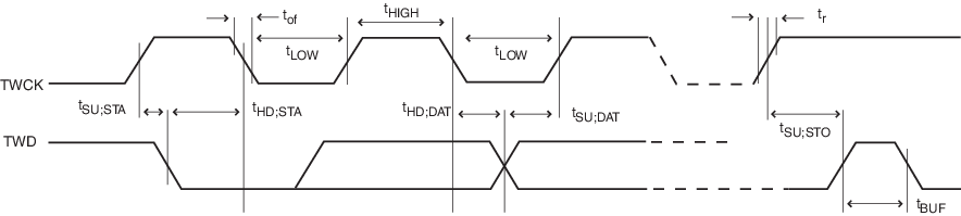
For additional information on timing symbols, refer to the figure below.
| Symbol | Parameter | Condition | Min. | Max. | Unit |
|---|---|---|---|---|---|
| VIL | Low-level Input Voltage | – | -0.3 | 0.3 VDDIO | V |
| VIH | High-level Input Voltage | – | 0.7 × VDDIO | VCC + 0.3 | V |
| Vhys | Hysteresis of Schmitt Trigger Inputs | – | 0.150 | – | V |
| VOL | Low-level Output Voltage | 3 mA sink current | – | 0.4 | V |
| tR | Rise Time for both TWD and TWCK | 20 + 0.1Cb(1)(2) | 300 | ns | |
| tOF | Output Fall Time from VIHmin to VILmax | 10 pF < Cb < 400 pF see the figure below |
20 + 0.1Cb(1)(2) | 250 | ns |
| Ci(1) | Capacitance for each I/O Pin | – | – | 10 | pF |
| fTWCK | TWCK Clock Frequency | – | 0 | 400 | kHz |
| RP | Value of Pull-up resistor | fTWCK ≤ 100 kHz | (VDDIO - 0.4V) ÷ 3mA | 1000ns ÷ Cb | Ω |
| fTWCK > 100 kHz | 300ns ÷ Cb | Ω | |||
| tLOW | Low Period of the TWCK clock | fTWCK ≤ 100 kHz | (3) | – | µs |
| fTWCK > 100 kHz | (3) | – | μs | ||
| tHIGH | High period of the TWCK clock | fTWCK ≤ 100 kHz | (4) | – | μs |
| fTWCK > 100 kHz | (4) | – | μs | ||
| tHD;STA | Hold Time (repeated) START Condition | fTWCK ≤ 100 kHz | tHIGH | – | μs |
| fTWCK > 100 kHz | tHIGH | – | μs | ||
| tSU;STA | Set-up time for a repeated START condition | fTWCK ≤ 100 kHz | tHIGH | – | μs |
| fTWCK > 100 kHz | tHIGH | – | μs | ||
| tHD;DAT | Data hold time | fTWCK ≤ 100 kHz | 0 | 3 × tCPMCK(5) | μs |
| fTWCK > 100 kHz | 0 | 3 ×tCPMCK(5) | μs | ||
| tSU;DAT | Data setup time | fTWCK ≤ 100 kHz | tLOW - 3 × tCPMCK(5) | – | ns |
| fTWCK > 100 kHz | tLOW - 3 × tCPMCK(5) | – | ns | ||
| tSU;STO | Setup time for STOP condition | fTWCK ≤ 100 kHz | tHIGH | – | μs |
| fTWCK > 100 kHz | tHIGH | – | μs | ||
| tHD;STA | Hold Time (repeated) START Condition | fTWCK ≤ 100 kHz | tHIGH | – | μs |
| fTWCK > 100 kHz | tHIGH | – | μs |
Notes:
- 1.Required only for fTWCK > 100 kHz.
- 2.Cb = capacitance of one bus line in pF. Per I2C standard, Cb max = 400pF.
- 3.The TWCK low period is defined as follows: tLOW = ((CLDIV × 2CKDIV) + 4) × tMCK.
- 4.The TWCK high period is defined as follows: tHIGH = ((CHDIV × 2CKDIV) + 4) × tMCK.
- 5.tCPMCK = MCK bus period
Figure 1. Two-wire Serial Bus Timing