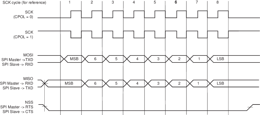
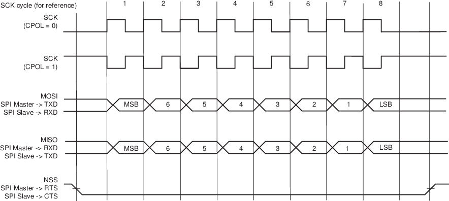
Up to nine data bits are successively shifted out on the TXD pin at each rising or falling edge (depending on CPOL and CPHA) of the programmed serial clock. There is no Start bit, no Parity bit and no Stop bit.
The number of data bits is selected using US_MR.CHRL and US_MR.MODE9. The nine bits are selected by setting the MODE9 bit regardless of the CHRL field. The MSB data bit is always sent first in SPI mode (Master or Slave).
Four combinations of polarity and phase are available for data transfers. The clock polarity is programmed using US_MR.CPOL. The clock phase is programmed using US_MR.CPHA. These two parameters determine the edges of the clock signal upon which data is driven and sampled. Each of the two parameters has two possible states, resulting in four possible combinations that are incompatible with one another. Thus, a master/slave pair must use the same parameter pair values to communicate. If multiple slaves are used and fixed in different configurations, the master must reconfigure itself each time it needs to communicate with a different slave.
| SPI Bus Protocol Mode | CPOL | CPHA |
|---|---|---|
| 0 | 0 | 1 |
| 1 | 0 | 0 |
| 2 | 1 | 1 |
| 3 | 1 | 0 |