The following are the two power supply nodes for SerDes.
- 1.SERDES_x_VDDAPLL
- 2.SERDES_x_PLL_VDDA
Figure 1. Filter Circuit for SerDes PLL Power
Supply

- C1 and R1 must be placed near the device.
- C2 must to be placed under the BGA via. The capacitor pad to via trace must be as small as possible.
Apart from this, a precision resistor (1.2 K) is placed between the SERDES_x_REXT and SERDES_x_REFRET pins. This resistor must be placed near the BGA via of SERDES_x_REXT pin. Any aggressive signal traces must be kept away from this resistor to avoid unwanted noise from coupling into this critical circuit. A sample placement is shown in the following figure.
Figure 2. Component Between 1.2 K Resistor and K6 Pin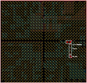
For more information about R1, C1, and C2, see Design Considerations.