Figure 1. SWD Interface Signals
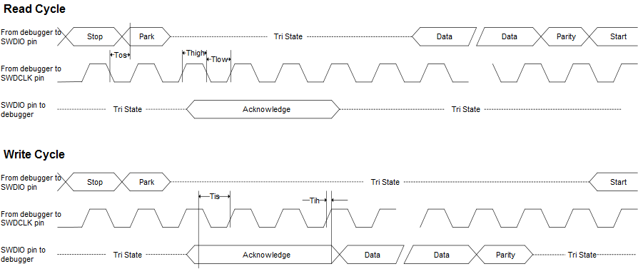
| Symbol | Parameter | Conditions | Min. | Max. | Units |
|---|---|---|---|---|---|
| Thigh | SWDCLK High period | VVDDIO from 3.0 V to 3.6 V, maximum external capacitor = 40 pF | 10 | 500000 | ns |
| Tlow | SWDCLK Low period | 10 | 500000 | ||
| Tos | SWDIO output skew to falling edge SWDCLK | -5 | 5 | ||
| Tis | Input Setup time required between SWDIO | 4 | - | ||
| Tih | Input Hold time required between SWDIO and rising edge SWDCLK | 1 | - |
Note:
- 1.These values are based on simulation. These values are not covered by test limits in production or characterization.