The analog voltage source must be able to
charge the sample and hold (S/H) capacitor in the ADC in order to achieve maximum accuracy.
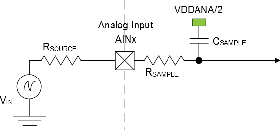
Seen externally the ADC input consists of a resistor (
RSAMPLE
) and a capacitor (
CSAMPLE
). In addition, the source resistance (
RSOURCE
) must be taken into account when calculating the required
sample and hold time. The figure below shows the ADC input channel equivalent circuit.
Figure 1. ADC Input
To achieve n bits of accuracy, the
CSAMPLE
capacitor must be charged at least to a voltage of
VCSAMPLE≥VIN×1−2−n+1
The minimum sampling time
tSAMPLEHOLD
for a given
RSOURCE
can be found using this formula:
tSAMPLEHOLD≥RSAMPLE+RSOURCE×CSAMPLE×n+1×ln2
for a 12 bits accuracy:
tSAMPLEHOLD≥RSAMPLE+RSOURCE×CSAMPLE×9.02
where
tSAMPLEHOLD=12×fADC