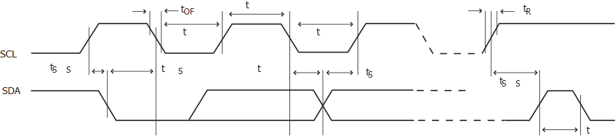
The following table describes the requirements for devices connected to the I2C Interface Bus. Timing symbols refer to the figure below.
Figure 1. I2C Interface Bus Timing
| Symbol | Parameter | Conditions | Min. | Typ. | Max. | Units |
|---|---|---|---|---|---|---|
| tR | Rise time for both SDA and SCL(3) | - | - | 300 | ns | |
| tOF | Output fall time from VIHmin to VILmax (3) | 10pF < Cb(2) < 400pF | 7.0 | 10.0 | 50.0 | |
| tHD;STA | Hold time (repeated) START condition | fSCL > 100kHz, Master | tLOW-9 | - | - | |
| tLOW | Low period of SCL Clock | fSCL > 100kHz | 113 | - | - | |
| tBUF | Bus free time between a STOP and a START condition | fSCL > 100kHz | tLOW | - | - | |
| tSU;STA | Setup time for a repeated START condition | fSCL > 100kHz, Master | tLOW+7 | - | - | |
| tHD;DAT | Data hold time | fSCL > 100kHz, Master | 9 | - | 12 | |
| tSU;DAT | Data setup time | fSCL > 100kHz, Master | 104 | - | - | |
| tSU;STO | Setup time for STOP condition | fSCL > 100kHz, Master | tLOW+9 | - | - | |
| tSU;DAT;rx | Data setup time (receive mode) | fSCL > 100kHz, Slave | 51 | - | 56 | |
| tHD;DAT;tx | Data hold time (send mode) | fSCL > 100kHz, Slave | 71 | 90 | 138 |
Notes: 1. These values are based on simulation. These values are not covered by test limits in production.
2. Cb = Capacitive load on each bus line. Otherwise noted, value of Cb set to 20pF.
3. These values are based on characterization. These values are not covered by test limits in production.