The ATA5835 consists of an analog front end, Digital Signal Processing (DSP) blocks, an 8-bit AVR sub-system and supporting modules, such as oscillators and power regulators. The following figure illustrates the hardware block diagram of the device.
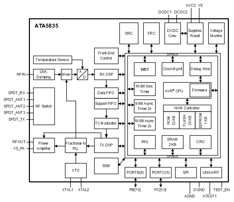
The receiver system is based on a low-IF architecture. The fractional-N PLL, which is clocked by the crystal oscillator (XTO), generates the Local Oscillator (LO) signal for the mixer. The RF signal is input at the pin RFIN, amplified by a Low-Noise Amplifier (LNA) and down-converted by the mixer to the Intermediate Frequency (IF) of approximately 250 kHz using the LO signal. A 10-dB IF amplifier with low-pass filter characteristic is used to achieve enhanced system sensitivity without affecting blocking performance. After the mixer, the IF signal is sampled using a high-resolution Analog-to-Digital Converter (ADC). A damping stage in the LNA can be activated to increase the large-signal immunity of the system.
Within the RX Digital Signal Processing (RX DSP), the received signal from the ADC is filtered by a digital channel filter and successively demodulated. Two data receive paths, path A and path B, are included in the RX DSP after the digital channel filter. In addition, the receive path can be configured to provide the digital output of an internal temperature sensor.
In the TXMode, the fractional-N PLL generates the TX frequency. The Power Amplifier (PA) generates a programmable RF output power signal at RFOUT. For more details on parameter number 10.00 output power of Electrical Characteristics, refer to the ATA5835 UHF ASK/FSK Transceiver Data Sheet (DS20005731). The FSK modulation is performed by changing the frequency setting of the fractional-N PLL dynamically by the TX Digital Signal Processing (TX DSP). Digital pre-emphasis and digital Gaussian shaping filter can be activated in the TX DSP to achieve higher data rates or reduce occupied bandwidth. The ASK modulation is performed by switching the power amplifier on and off. An ASK shaping filter is available to reduce the transmitted bandwidth of the modulated PA output signal. The shaping filter can also be used at the start and end of an FSK transmission.
The internal RF switch has three antenna connection pins that allow antenna diversity applications or channel-dependent filtering of the RF signal. The RF switch can switch any antenna signal to the RX pin SPDT_RX or the TX pin SPDT_TX. These signals must be routed to the RFIN and RFOUT pins via external matching networks, respectively. In a single antenna RX application, the antenna can directly be connected to the RFIN pin without using the RF switch.