When a voltage level imposed on a pin is sampled, it is first captured by the Sample-and-Hold capacitor (CIN). This ensures that the voltage does not change while the ADC samples the signal.
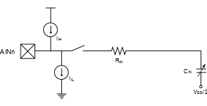
The time it takes to charge or discharge CIN to a certain voltage level is limited by the input resistance (RIN). The following equation shows the proportional relation between the time constant τ and the input impedance.
Refer to the Electrical Characteristics section in the data sheet for details on the input characteristics of the ADC.
The 12-bit resolution of the ADC (and optional gain) requires the impulse response of the input circuit settled to more than 99.9% of the final voltage to be certain the measurement will be correct. The following example calculations without gain and with 16x gain show how settled a signal needs to be for the ADC to sample correctly at 12-bit resolution.
The impulse response for the input circuit is given by the following equation.
Solving the two examples for VMSb where VIN is 100%, the following settling times are obtained.
The impedance of the external signal should also be taken into consideration when calculating the settling time, expanding the circuit into a more complex system as shown in the figure below.
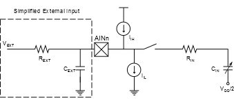
The characteristics of the external impedance determine how complex the settling time calculation will be. However, this is not covered by this technical brief.