Figure 1. 8-Pin PDIP, SOIC, DFN
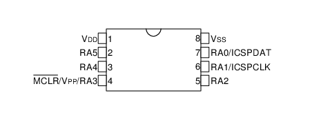
Figure 2. 14-Pin PDIP, SOIC, TSSOP
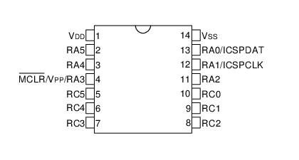
Figure 3. 16-Pin VQFN
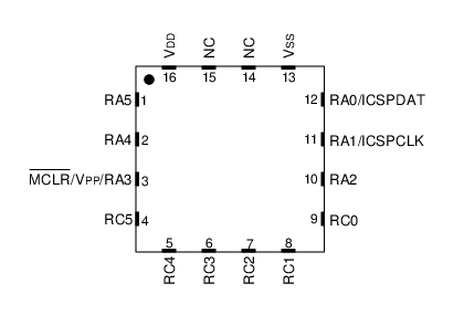
Note: It is recommended that the exposed
bottom pad be connected to VSS; however, it must not be the only
VSS connection to the device.
Figure 4. 20-Pin PDIP, SOIC, SSOP
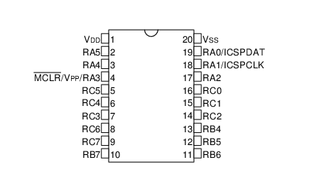
Figure 5. 20-Pin QFN
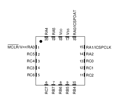
Note: It is recommended that the exposed
bottom pad be connected to VSS; however, it must not be the only
VSS connection to the device.
Figure 6. 28-Pin SPDIP, SOIC, SSOP
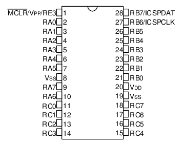
Figure 7. 28-Pin VQFN
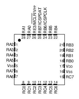
Figure 8. 40-Pin PDIP
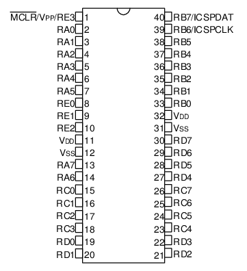
Figure 9. 40-Pin QFN
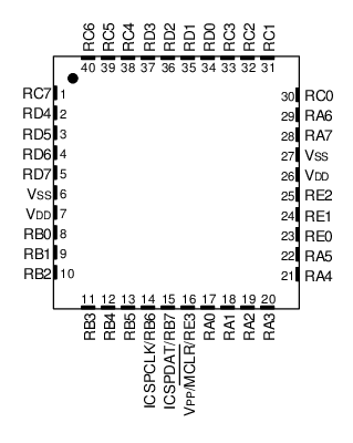
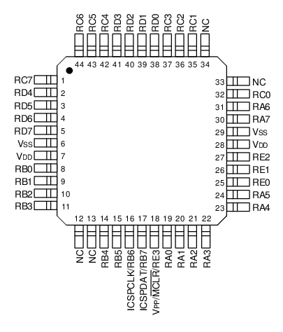
Figure 10. 44-Pin TQFP