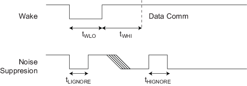
Figure 1. AC Timing Diagram: All Interfaces
| Parameter | Sym. | Direction | Min. | Typ. | Max. | Units | Conditions |
|---|---|---|---|---|---|---|---|
| Power-Up Delay(2) | tPU | To Crypto Device | 100 | — | — | µs | Minimum time between VCC > VCC min prior to start of tWLO. |
| Wake Low Duration | tWLO | To Crypto Device | 60 | — | — | µs | |
| Wake High Delay to Data Comm | tWHI | To Crypto Device | 1500 | — | — | µs | SDA should be stable high for this entire duration unless polling is implemented. SelfTest is not enabled at power-up. |
| Wake High Delay when SelfTest is Enabled | tWHIST | To Crypto Device | 20 | — | — | ms | SDA should be stable high for this entire duration unless polling is implemented. |
| High-Side Glitch Filter at Active | tHIGNORE_A | To Crypto Device | 45(1) | — | — | ns | Pulses shorter than this in width will be ignored by the device, regardless of its state when active. |
| Low-Side Glitch Filter at Active | tLIGNORE_A | To Crypto Device | 45(1) | — | — | ns | Pulses shorter than this in width will be ignored by the device, regardless of its state when active. |
| Low-Side Glitch Filter at Sleep | tLIGNORE_S | To Crypto Device | 15(1) | — | — | µs | Pulses shorter than this in width will be ignored by the device when in Sleep mode. |
| Watchdog Time-out | tWATCHDOG | To Crypto Device | 0.7 | 1.3 | 1.7 | s | Time from wake until device is forced into Sleep mode if Config.ChipMode[2] is 0. |
Notes:
- 1.These parameters are characterized, but not production tested.
- 2.The power-up delay will be significantly longer if power-on self test is enabled in the Configuration zone.