Figure 1. Block Diagram
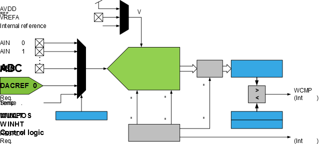
The analog input channel is selected by writing to the
MUXPOS bits in the MUXPOS (ADCn.MUXPOS) register. Any of the ADC input pins, GND, internal
Voltage Reference (VREF), or temperature sensor, can be selected as a
single-ended input to the ADC. The ADC is enabled by writing a ‘1’ to the
ADC ENABLE bit in the Control A (ADCn.CTRLA) register. The voltage reference and input
channel selections will not go into effect before the ADC is enabled. The ADC does not
consume power when the ENABLE bit in ADCn.CTRLA is ‘0’.
The ADC generates a 10-bit result that can be read from the Result (ADCn.RES) Register. The result is presented right-adjusted.