GPIO Input Characteristics
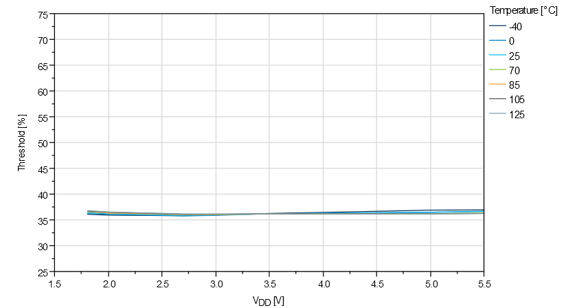
Figure 1. I/O Pin Input Hysteresis vs.
VDD
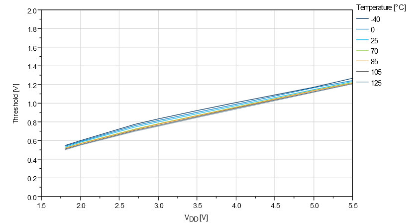
Figure 2. I/O Pin Input Threshold Voltage vs.
VDD (T = 25°C)
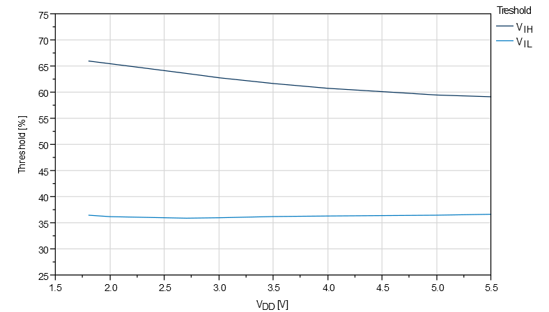
Figure 3. I/O Pin Input Threshold Voltage vs.
VDD (VIH)
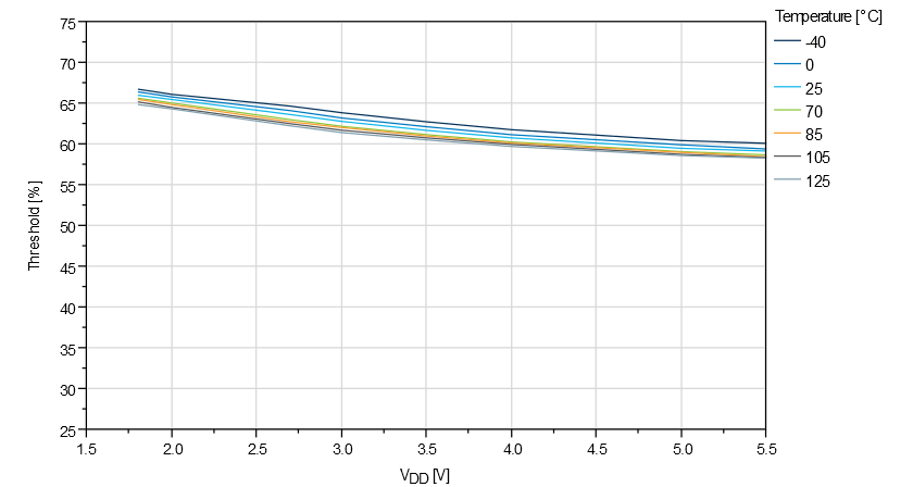
Figure 4. I/O Pin Input Threshold Voltage vs.
VDD (VIL)
GPIO Output Characteristics
Figure 5. I/O Pin Output Voltage vs. Sink
Current (VDD = 1.8V)
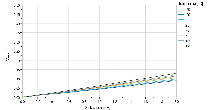
Figure 6. I/O Pin Output Voltage vs. Sink
Current (VDD = 3.0V)
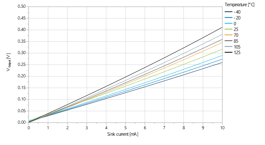
Figure 7. I/O Pin Output Voltage vs. Sink
Current (VDD = 5.0V)
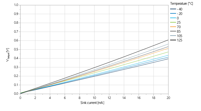
Figure 8. I/O Pin Output Voltage vs. Sink
Current (T = 25°C)
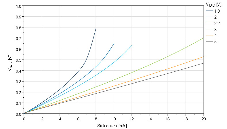
Figure 9. I/O Pin Output Voltage vs. Source
Current (VDD = 1.8V)
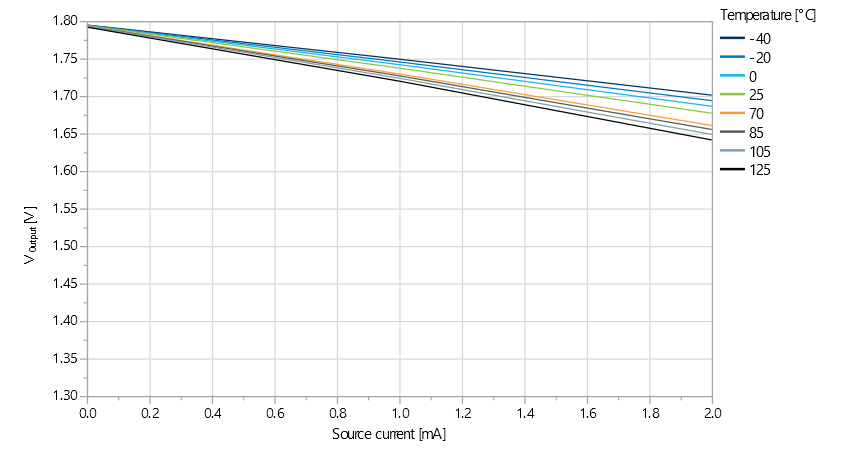
Figure 10. I/O Pin Output Voltage vs. Source
Current (VDD = 3.0V)
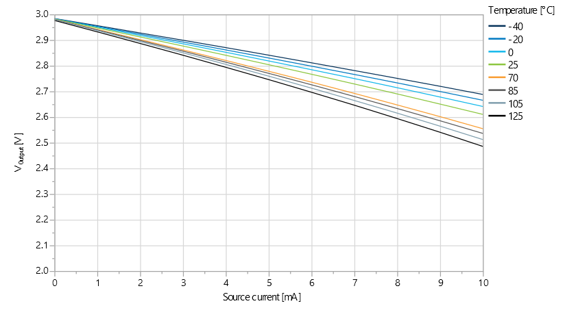
Figure 11. I/O Pin Output Voltage vs. Source
Current (VDD = 5.0V)
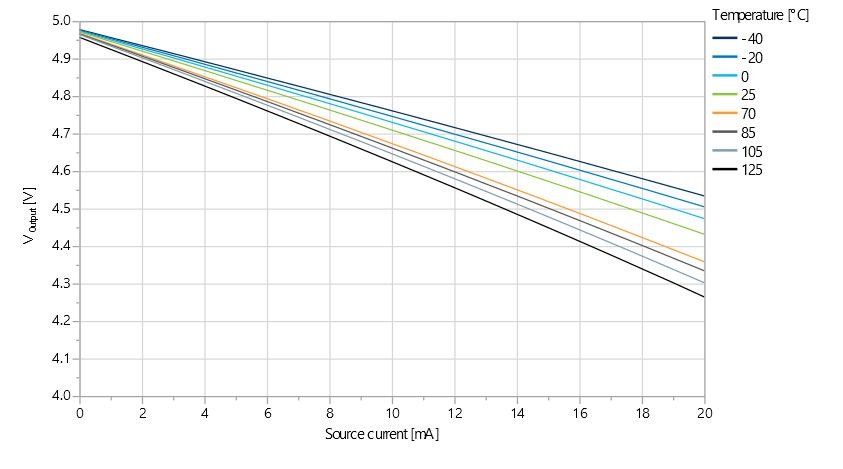
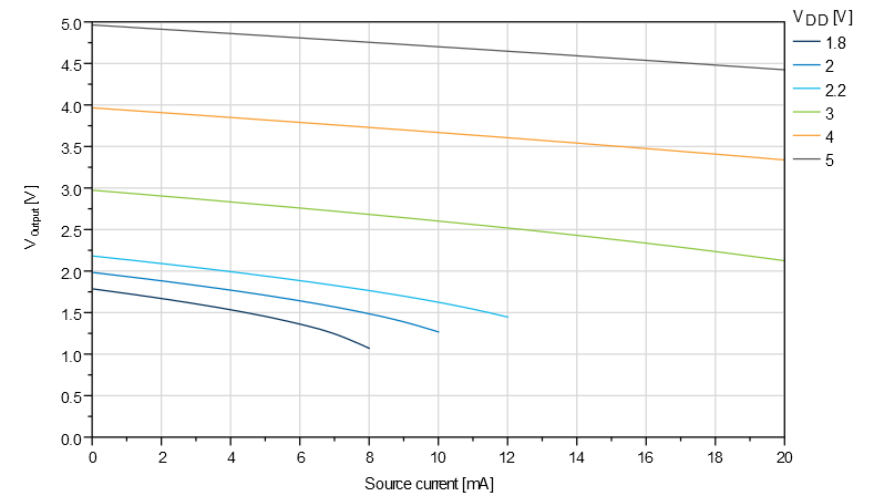
Figure 12. I/O Pin Output Voltage vs. Source
Current (T = 25°C)
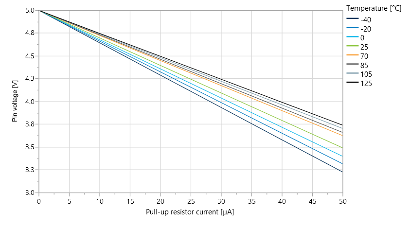
GPIO Pull-Up Characteristics
Figure 13. I/O Pin Pull-Up Resistor Current vs.
Input Voltage (VDD = 1.8V)
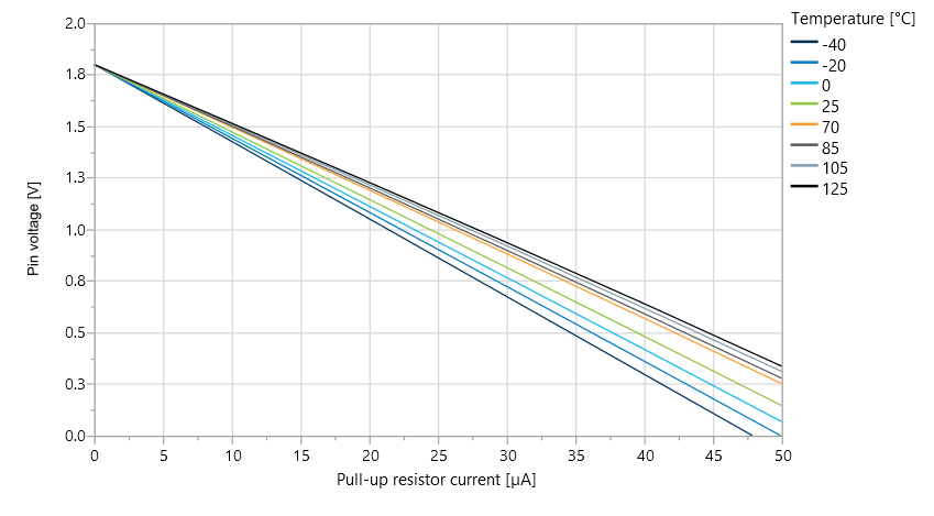
Figure 14. I/O Pin Pull-Up Resistor Current vs.
Input Voltage (VDD = 3.0V)
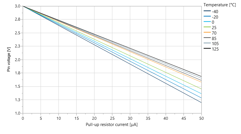
Figure 15. I/O Pin Pull-Up Resistor Current vs.
Input Voltage (VDD = 5.0V)