To generate this project using MPLAB Code Configurator (MCC) the next steps need to be followed:
- 1.Create a new MPLAB X IDE project for PIC18F47Q10.
- 2.Open the MCC from the toolbar (information about how to install the MCC plug-in can be found here).
- 3.Go to Project Resources →
System → System Module and make the following configurations:
- Oscillator Select: HFINTOSC
- HF Internal Clock: 4 MHz
- Clock Divider: 1
- In the Watchdog Timer Enable field in the WWDT tab, WDT Disabled has to be selected
- In the Programming tab, Low-Voltage Programming Enable has to be checked
- 4.From the Device Resources window, add
TMR2, MSSP1 and make the following configurations:
Timer2 Configuration:
- Enable Timer: checked
- Timer Clock tab
- Clock Source: HFINTOSC
- Clock Prescaler: 1:64
- Postscaler: 1:1
- Set 50 µs period in the Timer Period tab
MSSP1 Configuration:
- Serial Protocol: SPI
- Mode: Master
- SPI Mode: SPI Mode 0
- Input Data Sampled At: Middle
- Clock Source Selection: TMR2/2
- Actual Clock Frequency (Hz): 10000.00
- 5.Open Pin Manager → Grid
View window, select UQFN40 in the MCU package field, and make the
following pin configurations:
- Set Port C pin 6 (RC6) as output for Slave Select 1 (SS 1)
- Set Port C pin 7 (RC7) as output for Slave Select 2 (SS 2)
The SCK, SDO and SDI pins appear alongside the MSSP1 peripheral and have their direction preset.
Figure 1. Pin Mapping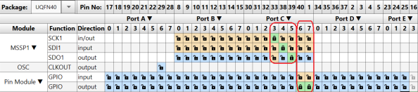
- 6.Click Pin Module in the Project
Resources and set the custom names SS pins:
- Rename RC6 to Slave1
- Rename RC7 to Slave2
- 7.Click Generate in the Project Resources tab.
- 8.In the
main.cfile generated by MCC, add the following code:- Control of Slave devices
- Data transmission
uint8_t writeData = 1;          /* Data that will be transmitted */
uint8_t receiveData;            /* Data that will be received */

void main(void)
{
    // Initialize the device
    SYSTEM_Initialize();

    while (1)
    {
        SPI1_Open(SPI1_DEFAULT);
        Slave1_SetLow();
        receiveData = SPI1_ExchangeByte(writeData);
        Slave1_SetHigh();
        SPI1_Close();

        SPI1_Open(SPI1_DEFAULT);
        Slave2_SetLow();
        receiveData = SPI1_ExchangeByte(writeData);
        Slave2_SetHigh();
        SPI1_Close();
    }
}