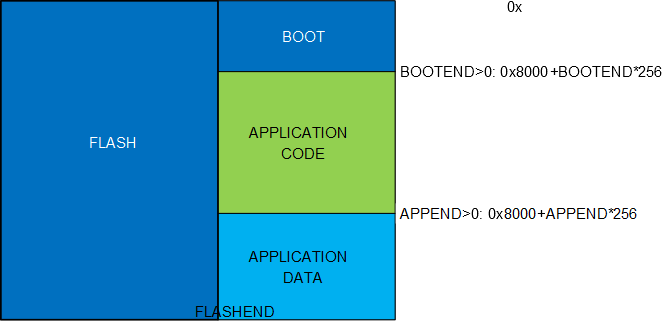
The ATtiny202/204/402/404/406 contains 2/4 KB on-chip in-system reprogrammable Flash memory for program storage. Since all AVR instructions are 16 or 32-bit wide, the Flash is organized with 16-bit data width. For write protection, the Flash program memory space can be divided into three sections (see the illustration below): Bootloader section, Application code section, and Application data section, with restricted access rights among them.
The Program Counter (PC) is 11-bit wide to address the whole program memory. The procedure for writing Flash memory is described in detail in the documentation of the Nonvolatile Memory Controller (NVMCTRL) peripheral.
The entire Flash memory is mapped in the memory space and is accessible with
normal LD/ST instructions as well as the
LPM instruction. For LD/ST
instructions, the Flash is mapped from address 0x8000. For the LPM
instruction, the Flash start address is 0x0000.
The ATtiny202/204/402/404/406 also has a CRC peripheral that is a host on the bus.