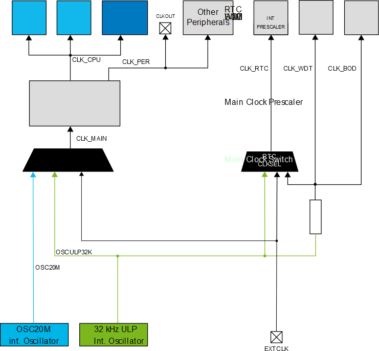
Figure 1. CLKCTRL Block Diagram
Note: The availability of the CLKOUT pin depends on the pin count of the device. See
section I/O Multiplexing and Considerations for an
overview of which pins are available for each device represented in this data sheet.
The clock system consists of the Main Clock and other asynchronous clocks:
- Main Clock
This clock is used by the CPU, RAM, Flash, the I/O bus, and all peripherals connected to the I/O bus. It is always running in Active and Idle sleep modes and can be running in Standby sleep mode if requested.
The main clock CLK_MAIN is prescaled and distributed by the Clock Controller:- CLK_CPU is used by the CPU, SRAM and the NVMCTRL peripheral to access the nonvolatile memory
- CLK_PER is used by all peripherals that are not listed under asynchronous clocks
- Clocks running asynchronously to the Main Clock domain:
- CLK_RTC is used by the RTC/PIT. It will be requested when the RTC/PIT is enabled. The clock source for CLK_RTC must only be changed if the peripheral is disabled.
- CLK_WDT is used by the WDT. It will be requested when the WDT is enabled.
- CLK_BOD is used by the BOD. It will be requested when the BOD is enabled in Sampled Mode.
The clock source for the Main Clock domain is configured by writing to the Clock Select (CLKSEL) bits in the Main Clock Control A (CLKCTRL.MCLKCTRLA) register. The asynchronous clock sources are configured by registers in the respective peripheral.