To protect the device from voltages above VCC and below GND, the AVR has internal clamping diodes on the I/O pins (see Figure 1). The diodes are connected from the pins to VCC and GND and keep all input signals within the AVR’s operating voltage (see the figure below). Any voltage higher than VCC + 0.5V will be forced down to VCC + 0.5V (0.5V is the voltage drop over the diode) and any voltage below GND - 0.5V will be forced up to GND - 0.5V.
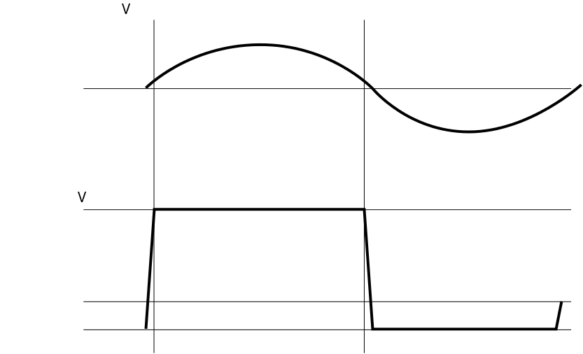
By adding a large resistor in series, these diodes can be used to convert a high voltage sinus signal down to a low voltage square wave signal, with amplitude within the AVR’s operating voltage ±0.5V. The diodes will thus clamp the high voltage signal down to the AVR’s operating voltage.
As the square wave signal is in phase with the AC mains, using the falling edge will tell very accurately where the zero crossing happens. By using this signal the AVR can be programmed to be a very accurate zero cross detector with a very small and interrupt-driven code.
The square wave is the mains signal with its tops cut off and will have the same voltage from VCC - 0.5V to VCC + 0.5V as the mains signal (see the figure below). When the square wave triggers the AVR’s falling edge interrupt at around VCC/2, the mains amplitude will also be at VCC/2 and just before a zero crossing. If this is done on a falling edge the AVR will get an interrupt just before the zero crossing and will have time to start a zero crossing action at the actual crossing point. The interrupt will be triggered at around VCC/2, as this is the middle of the AVR’s logical threshold voltage.
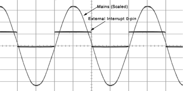
The signal is connected to the External Interrupt 0-pin, which makes it possible to place the zero cross detection routine in an interrupt routine and make the detection fully interrupt driven. The second figure below shows an oscilloscope screen-shot of the actual input signal. Note that the Mains signal is scaled and the rising edge of the external int 0-pin is the same edge as for the Mains, because of the scaling, the Mains edge looks like it appears after the external int 0 edge.
The series input resistor is a 1MΩ resistor. It is not recommended that the clamping diodes are conducting more than maximum 1mA, and 1MΩ will then allow a maximum voltage of approximately 1,000V.
Any voltage higher than 1,000V would probably be spikes or surges. The clamping diodes are able to handle spikes for a short period of time but not surges. The application note will not go into how to protect against surges, but simply recommend implementing protection against surges in the design.
Most resistors have an upper maximum voltage limit. Make sure that the resistors used in the application can handle the highest possible AC mains voltage, including high voltage spikes.
For systems with lower mains voltages the resistor value can be changed, but in general it should be able to sense 110 - 240V AC systems without any problems.
The 1MΩ resistor in series to mains GND will ensure a correct ground potential for the application.