Operating conditions:
- VDD = 3V, unless otherwise specified
- Oscillator frequencies above speed specification must be divided, so the CPU clock is always within specification
| Symbol | Description | Condition | Min. | Typ. | Max. | Unit | |
|---|---|---|---|---|---|---|---|
| fOSC20M | Factory calibration frequency | FREQSEL = 0x01 |
TA = 25°C, 3.0V | - | 16 | - | MHz |
FREQSEL = 0x02 |
- | 20 | - | ||||
| fCAL | Frequency calibration range | OSC20M FREQSEL = 0x01 |
14.5 | - | 17.5 | MHz | |
OSC20M FREQSEL = 0x02 |
18.5 | - | 21.5 | MHz | |||
| ETOTAL | Total error with 16 MHz and 20 MHz frequency selection | From target frequency | TA = 25°C, 3.0V | -1.5 | - | 1.5 | % |
| TA = [0, 70]°C, VDD = [1.8, 3.6]V | -2.0(1) | - | 2.0(1) | % | |||
| Full operation range | -3.5 | - | 3.5 | ||||
| ΔfOSC20M | Calibration step size | - | 0.75 | - | % | ||
| DOSC20M | Duty cycle | - | 50 | - | % | ||
| tstartup | Start-up time | Within 2% accuracy | - | 12 | - | µs | |
Note:
- 1.These values are based on characterization and are not covered by production test limits.
| Symbol | Description | Condition | Min. | Typ. | Max. | Unit |
|---|---|---|---|---|---|---|
| fOSCULP32K | Factory calibration frequency | - | 32.768 | - | kHz | |
| Factory calibration accuracy | TA = 25°C, 3.0V | -3 | - | 3 | % | |
| ETOTAL | Total error from target frequency | TA = [0, 70]°C, VDD = [1.8, 3.6]V | -10(1) | - | +10(1) | % |
| Full operation range | -20 | - | +20 | |||
| DOSCULP32K | Duty cycle | - | 50 | - | % | |
| tstartup | Start-up time | - | 250 | - | µs |
Note:
- 1.These values are based on characterization and are not covered by production test limits.
| Symbol | Description | Condition | Min. | Typ. | Max. | Unit |
|---|---|---|---|---|---|---|
| fout | Frequency | - | 32.768 | - | kHz | |
| tstartup | Start-up time | CL = 7.5 pF | - | 300 | - | ms |
| CL | Crystal load capacitance | 7.5(1) | - | 12.5(1) | pF | |
| ESR | Equivalent Series Resistance - Safety Factor=3 | CL = 7.5 pF | - | - | 80(1) | kΩ |
| CL = 12.5 pF | - | - | 40(1) |
Note:
- 1.This parameter is for design guidance only. Not production tested.
Figure 1. External Clock Waveform Characteristics
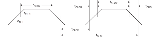
| Symbol | Description | Condition | VDD=[1.8, 5.5]V | VDD=[2.7, 5.5]V | VDD=[4.5, 5.5]V | Unit | |||
|---|---|---|---|---|---|---|---|---|---|
| Min. | Max. | Min. | Max. | Min. | Max. | ||||
| fCLCL | Frequency | 0 | 5.0 | 0.0 | 10.0 | 0.0 | 20.0 | MHz | |
| tCLCL | Clock Period | 200 | - | 100 | - | 50 | - | ns | |
| tCHCX(1) | High Time | 80 | - | 40 | - | 20 | - | ns | |
| tCLCX(1) | Low Time | 80 | - | 40 | - | 20 | - | ns | |
| tCLCH(1) | Rise Time (for maximum frequency) | - | 40 | - | 20 | - | 10 | ns | |
| tCHCL(1) | Fall Time (for maximum frequency) | - | 40 | - | 20 | - | 10 | ns | |
| ΔtCLCL(1) | Change in period from one clock cycle to the next | - | 20 | - | 20 | - | 20 | % | |
Note:
- 1.This parameter is for design guidance only. Not production tested.