The device must operate within the ratings listed in this
section for all other electrical characteristics and typical characteristics of the device to
be valid.
| Symbol | Description | Condition | Min. | Max. | Unit |
|---|---|---|---|---|---|
| VDD | Operating supply voltage | Industrial | 1.8(1,2) | 5.5 | V |
| VAO - Auto Grade and Extended Operating temperature range | 2.7(2,3) | 5.5 | V | ||
| TA | Operating temperature range | Extended | -40 | 125 | °C |
| Industrial | -40 | 85 |
Notes:
- 1.Operation is ensured down to 1.8V or BOD triggering level VBOD when BOD is active.
- 2.During Chip Erase, the BOD is forced ON. If the supply voltage VDD is below the configured VBOD, the erase attempt will fail.
- 3.Operation is ensured down to 2.7V or BOD triggering level VBOD when BOD is active.
| Symbol | Description | Condition | Min. | Max. | Unit | |
|---|---|---|---|---|---|---|
| fCLK_CPU | Nominal operating system clock frequency | TA = [-40, 85]°C |
VDD = [1.8, 2.7]V(1,4) |
0 | 5 | MHz |
| VDD = [2.7, 4.5]V(2) | 0 | 10 | ||||
| VDD = [4.5, 5.5]V(3) | 0 | 20 | ||||
| TA = [85, 125]°C | VDD = [2.7, 4.5]V(2) | 0 | 8 | |||
|
VDD = [4.5, 5.5]V(3) |
0 | 16 | ||||
Notes:
- 1.Operation is ensured down to BOD triggering level, VBOD with BODLEVEL0.
- 2.Operation is ensured down to BOD triggering level, VBOD with BODLEVEL2.
- 3.Operation is ensured down to BOD triggering level, VBOD with BODLEVEL7.
- 4.These specifications do not apply to automotive range parts (-VAO).
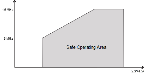
The maximum CPU clock frequency depends on VDD. As shown in the figure below, the Maximum Frequency vs. VDD is linear between 1.8V < VDD < 2.7V and 2.7V < VDD < 4.5V.
Figure 1. Maximum Frequency vs. VDD for
[-40, 85]°C

Figure 2. Maximum Frequency vs. VDD for
[85, 125]°C