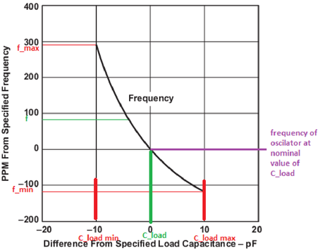
Crystal manufacturers specify an external capacitive load to apply to the crystal. Mismatching the capacitive load will result in lower accuracy of the crystal, or even failure to oscillate. A typical characteristic curve of frequency versus load capacitance, as can be found in a crystal oscillator data sheet, is shown in Figure 1.
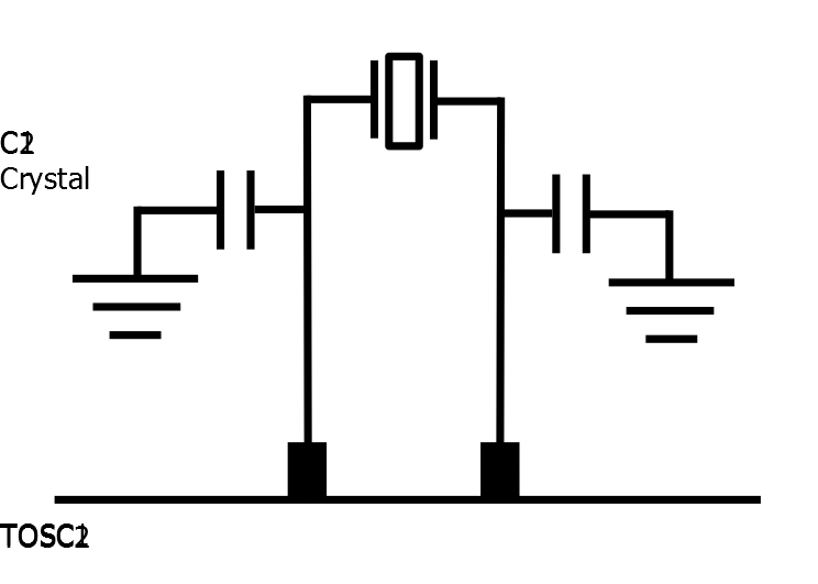
Multiple sources contribute to the load capacitance in a crystal circuit:
- The PCB parasitic capacitance, which is capacitance between PCB traces.
- The MCU parasitic capacitance. Refer to the electrical characteristics of the device data sheet for further details.
- The mounted capacitors C1 and C2, which are placed between the TOSC1 pin of the MCU and GND, and the TOSC2 pin of the MCU and GND, respectively.
When calculating the value of C1 and C2, the MCU parasitic capacitance and the PCB parasitic capacitance must be taken into account. PCB parasitic capacitance is dependent on the PCB design. For example, the choice of track length and width will impact the capacitance. For more information on best practices on this, refer to AVR4100: Selecting and testing 32.768 kHz crystal oscillators for Atmel AVR microcontrollers.
All components are subject to manufacturing tolerance. This means that correctly selecting C1 and C2 will not ensure an identical accuracy for all units produced. Because of this, software-based compensation must be performed to achieve optimal precision in timekeeping.