The standard PWM function described in this section is available and identical for all CCP modules. It generates a PWM signal on the CCPx pin with up to 10 bits of resolution. The period, duty cycle, and resolution are controlled by the following registers:
- Even numbered TxPR (T2PR) registers
- Even numbered TxCON (T2CON) registers
- 16-bit CCPRx registers
- CCPxCON registers
It is required to have FOSC/4 as the clock input to T2TMR for correct PWM operation. The following figure shows a simplified block diagram of PWM operation.
Figure 1. Simplified PWM Block Diagram
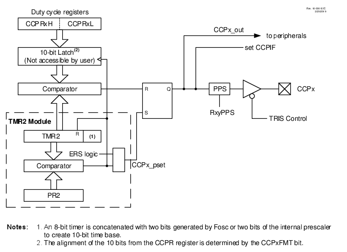
Important: The corresponding TRIS bit must be cleared to enable the PWM output on the CCPx pin.