The Universal Synchronous and Asynchronous serial Receiver and Transmitter (USART) is a highly-flexible serial communication device. A simplified block diagram of the USART Transmitter is shown in the figure below. CPU accessible I/O Registers and I/O pins are shown in bold.
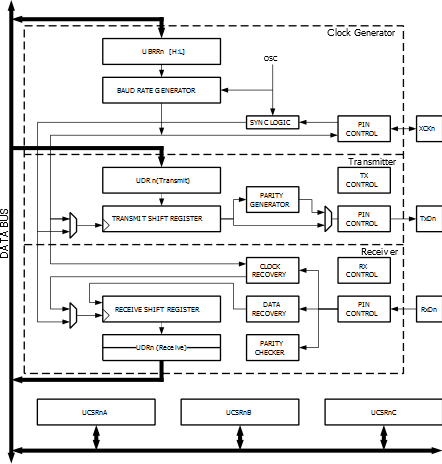
The dashed boxes in the block diagram separate the three main parts of the USART (listed from the top): Clock generator, Transmitter and Receiver. Control Registers are shared by all units. The clock generation logic consists of synchronization logic for external clock input used by synchronous slave operation, and the baud rate generator. The XCK (transfer clock) pin is only used by synchronous transfer mode. The Transmitter consists of a single write buffer, a serial Shift Register, Parity Generator and control logic for handling different serial frame formats. The write buffer allows a continuous transfer of data without any delay between frames. The Receiver is the most complex part of the USART module due to its clock and data recovery units. The recovery units are used for asynchronous data reception. In addition to the recovery units, the Receiver includes a parity checker, control logic, a Shift Register and a two level receive buffer (UDR). The Receiver supports the same frame formats as the Transmitter, and can detect Frame Error, Data OverRun and Parity Errors.