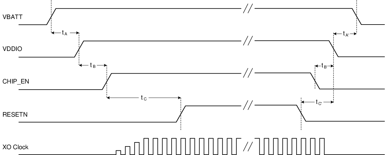
The power-up/down sequence for ATWINC15x0-MR210xB is shown in the following figure. The timing parameters are shown in the following table.
Figure 1. Power Up/Down Sequence
| Parameter | Min. | Max. | Units | Description | Notes |
|---|---|---|---|---|---|
| tA | 0 | — | ms | VBATT rise to VDDIO rise | VBATT and VDDIO can rise simultaneously or can be tied together. VDDIO must not rise before VBATT. |
| tB | 0 | — | ms | VDDIO rise to CHIP_EN rise | CHIP_EN must not rise before VDDIO. CHIP_EN must be driven high or low, not left floating. |
| tC | 5 | — | ms | CHIP_EN rise to RESETN rise | This delay is needed because the XO clock must stabilize before RESETN removal. RESETN must be driven high or low, not left floating. |
| tA’ | 0 | — | ms | VDDIO fall to VBATT fall | VBATT and VDDIO can fall simultaneously or can be tied together. VBATT must not fall before VDDIO. |
| tB’ | 0 | — | ms | CHIP_EN fall to VDDIO fall | VDDIO must not fall before CHIP_EN. CHIP_EN and RESETN can fall simultaneously. |
| tC’ | 0 | — | ms | RESETN fall to VDDIO fall | VDDIO must not fall before RESETN. RESETN and CHIP_EN can fall simultaneously. |