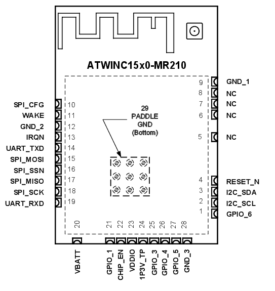
The following figure illustrates the ATWINC15x0-MR210xB module pin out. This module has an exposed ground pad that must be connected to the system board ground.
Figure 1. Pin Diagram
| Pin # | Name | Type | Description | Programmable Pull Up Resistor |
|---|---|---|---|---|
| 1 | GPIO_6 | I/O | General purpose I/O(1). | Yes |
| 2 | I2C_SCL | I/O | I2C Client Clock. Currently used only for development debugging. Leave unconnected. It is recommended to add Test Point to this pin. | Yes |
| 3 | I2C_SDA | I/O | I2C Client Data. Currently used only for development debugging. Leave unconnected. It is recommended to add Test Point to this pin. | Yes |
| 4 | RESET_N | I | Active-Low Hard Reset. When this pin is asserted low, the module is set to the reset state. When this pin is asserted high, the module comes out of reset and functions normally. Connect to a host output that defaults low at power up. If the host output is tri-stated, add a 1 MΩ pull-down resistor to ensure a low level at power-up. | No |
| 5 | NC | — | No connect. | — |
| 6 | NC | — | No connect. | — |
| 7 | NC | — | No connect. | — |
| 8 | NC | — | No connect. | — |
| 9 | GND_1 | — | GND. | — |
| 10 | SPI_CFG | I | Tie to VDDIO through a 1 MΩ resistor to enable the SPI interface. | No |
| 11 | WAKE | I | Host Wake control. Can be used to wake up the module from Doze mode. Current FW implementation makes use of IRQ to wake up the host. | Yes |
| 12 | GND_2 | — | GND. | — |
| 13 | IRQN | O | ATWINC15x0-MR210xB Device Interrupt output. Connect to host interrupt input pin. | Yes |
| 14 | UART_TXD | O | UART Transmit Output from
ATWINC15x0-MR210xB. Added for debugging and testing only. |
Yes |
| 15 | SPI_MOSI | I | SPI MOSI (Host Out, Client In) pin. | Yes |
| 16 | SPI_SSN | I | SPI Client Select. Active-low. | Yes |
| 17 | SPI_MISO | O | SPI MISO (Host In, Client Out) pin. | Yes |
| 18 | SPI_SCK | I | SPI Clock. | Yes |
| 19 | UART_RXD | I | UART Receive input to ATWINC15x0-MR210xB. Added for debugging and testing only. |
Yes |
| 20 | VBATT | — | Battery power supply. | — |
| 21 | GPIO_1 | I | General Purpose I/O(1). | Yes |
| 22 | CHIP_EN | I | Module enable. High level enables the module; low level places the module in Power-Down mode. Connect to a host output that defaults low at power-up. If the host output is tri-stated, add a 1 MΩ pull-down resistor to ensure a low level at power-up. | No |
| 23 | VDDIO | — | I/O Power Supply. Must match the host I/O voltage. | — |
| 24 | 1P3V_TP | — | 1.3V VDD Core Test Point. Decouple with the 10 µF and 0.01 µF to the GND. Close to the pin. | — |
| 25 | GPIO_3 | I/O | General purpose I/O(1). | Yes |
| 26 | GPIO_4 | I/O | General purpose I/O(1). | Yes |
| 27 | GPIO_5 | I/O | General purpose I/O(1). | Yes |
| 28 | GND_3 | — | GND. | — |
| 29 | PADDLE GND | — | GND. | — |
Note:
- 1.Usage of the GPIO functionality is not supported by the WINC15x0 FW. The datasheet will be updated once the support for this feature is added.