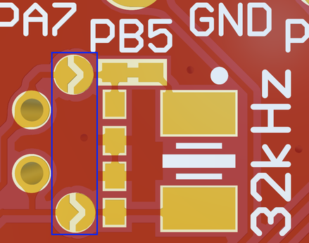
The ATtiny3217 Curiosity Nano Board has a 32.768 kHz crystal footprint made for standard 3.2mm by 1.5mm surface mount crystals with two terminals.
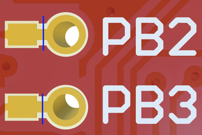
The crystal footprint is not connected to the ATtiny3217 by default, as the GPIOs are routed out to the edge connector. To use the crystal, some hardware modifications are required. The two I/O lines routed to the edge connector must be disconnected to reduce the chance of contention to the crystal, and to remove excessive capacitance on the lines. This can be done by cutting the two straps on the bottom side of the board, marked PB2 and PB3 as shown in the figure below. Next, short circuit each of the circular solder points next to the crystal on the top side of the board, the easiest way is to solder a solder tin blob across the footprint.
 |
 |
A crystal with 7pF equivalent load capacitance and 70kΩ ESR (XC200) and one 10pF external matching capacitor (C203), and one 13pF external matching capacitor (C204) have been tested to yield good results on this board. See the Assembly Drawing for footprint locations.
| ATtiny3217 Pin | Function | Shared Functionality |
|---|---|---|
| PB3 | TOSC1 (input) | Edge connector |
| PB2 | TOSC2 (output) | Edge connector |