These accesses consist of a one-byte op_code followed by an address phase. The address phase is two bytes of address for 25xx256 devices and three bytes of address for the SST25VFxxxx devices.
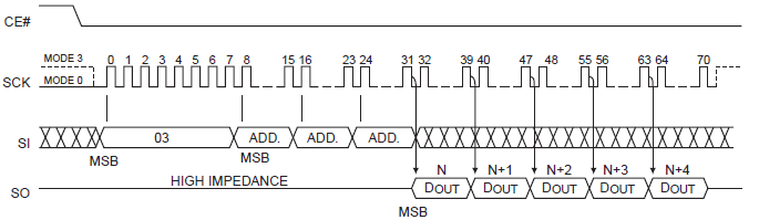
The device is selected by pulling CE low. The 8-bit READ instruction is transmitted to the device followed by the address. After the correct READ instruction and address are sent, the data stored in the memory at the selected address is shifted out on the SO pin. The data stored in the memory at the next address can be read sequentially by continuing to provide clock pulses. The internal address pointer is automatically incremented to the next higher address after each byte of data is shifted out. When the highest address is reached, the address counter rolls over to address 0000h allowing the read cycle to be continued indefinitely. The read operation is terminated by raising the CE pin.