When writing the WPR, data bit 7 through 4 are used to ensure that a write operation was
intentional. For all write operations to the WPR, bit 6 must be a logic
‘1’ as seen in Table 3.
Additionally, data bit 5 must be set in accordance with the D0 bit value (WPRL) as noted
below. If the WPR is to remain unlocked, then the upper nibble sent during the write
operation would be 4h and D0 must be a logic ‘0’, whereas if the WPR is
to be permanently locked, the upper nibble would need to be 6h and D0 must be a logic
‘1’. A mismatch of D5 and the WPRL bit will cause the write cycle
to abort.
1), the write cycle will not execute and the device will be ready
for a new operation.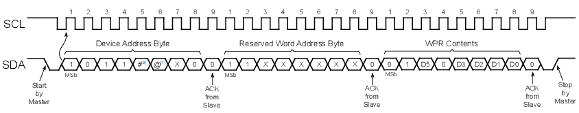
- 1.
For the AT24CSW04X, the @ indicates the A1 Address bit which is managed by the ordering code of the device (see Table 3). For the AT24CSW08X, the @ indicates the A9 address bit.
- 2.# indicates the hardware address value which is managed by the ordering code of the device (see Table 3 and Table 4).