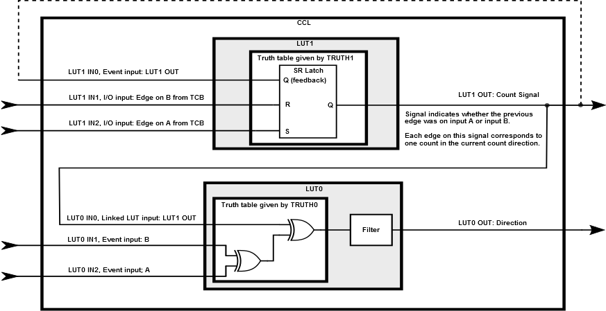
The Configurable Custom Logic (CCL) module creates the count signal and the direction signal by acting as glue logic. The module contains a number of look-up tables (LUTs), which each can perform a logic operation based on its three inputs. The inputs are selectable from a large number of both internal and external signals.
For this application note two LUTs are utilized; one for each of the generated signals. The basic behavior of each LUT is given by its TRUTH register. The TRUTH register defines a truth table for the LUT that maps each logical combination of the three inputs to a true or false (high or low) output value. Each bit in the TRUTH register represents one of the eight possible input value combinations, and the value of the bit represents the LUT output value for that combination.
The figure below shows an overview of the Configurable Custom Logic (CCL) configuration for this application.
LUT1 Setup
LUT1 is used to generate a signal, which indicates which of the quadrature input channels contain the last detected edge. Each edge of this signal corresponds to a quadrature count. This functionality is equivalent to an SR latch that takes the output of an edge detector connected to each quadrature signal as an input. The truth table for a generic active-high SR latch is included below.
| S | R | OUT |
|---|---|---|
0 |
0 |
Hold state (no change) |
0 |
1 |
0 (Clear) |
1 |
0 |
1 (Set) |
1 |
1 |
Forbidden state |
- The current output of the LUT
- Signal strobe indicating an edge on B
- Signal strobe indicating an edge on A
The LUT output is fed back to IN0 via the event system.
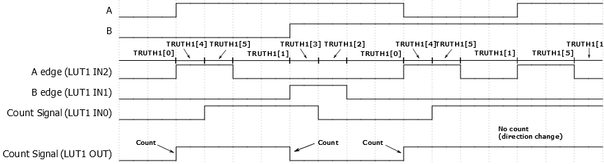
Implementing the SR latch functionality described above is done by
setting up the TRUTH1 register as indicated in the table below, where “edge on A”
acts as Set and “edge on B” acts as Clear. The bit combination
‘0b00110010’ given by THRUTH1[0-7] in the OUT column,
equivalent to the hexadecimal value 0x32, is the resulting 8-bit value to write to
the TRUTH1 register.
| IN[2] | IN[1] | IN[0] | OUT (TRUTH1) | Corresponding SR Latch Output |
|---|---|---|---|---|
| Edge on A | Edge on B | Count Signal Feedback | Count Signal Output | |
0 |
0 |
0 |
0 (TRUTH1[0]) |
Hold state (no change) |
0 |
0 |
1 |
1 (TRUTH1[1]) |
Hold state (no change) |
0 |
1 |
0 |
0 (TRUTH1[2]) |
0 (Clear) |
0 |
1 |
1 |
0 (TRUTH1[3]) |
0 (Clear) |
1 |
0 |
0 |
1 (TRUTH1[4]) |
1 (Set) |
1 |
0 |
1 |
1 (TRUTH1[5]) |
1 (Set) |
1 |
1 |
0 |
0 (TRUTH1[6]) |
Forbidden state |
1 |
1 |
1 |
0 (TRUTH1[7]) |
Forbidden state |
The waveform below shows the output signal for an example sequence of input signals, as well as the corresponding row in the LUT1 truth table for each input value combination. Additionally, the actual A and B input signals are included. The main purpose of the figure is to show the mapping between the LUT inputs and outputs. Pulse lengths on LUT1 IN0 and IN1, as well as the delay from LUT1 OUT to LUT1 IN0, have therefore been exaggerated for clarity.
LUT0 Setup
- Output from LUT1 indicating which channel contained the previous edge
- B
- A
As illustrated for LUT0 in the figure included initially, the direction signal is created by performing a series of two XOR operations. The first takes the A and B signals as inputs, while the second takes the count signal and the output from the first XOR as inputs. In order to configure the LUT as described, its TRUTH register needs to be set up according to the table below. The bit combination 0b10010110 given by THRUTH0[0-7] in the OUT column, equivalent to the hexadecimal value 0x96, is the resulting 8-bit value to write to the TRUTH0 register.
| IN[2] | IN[1] | IN[0] | OUT (TRUTH0) |
|---|---|---|---|
| A | B | Count Signal from LUT1 | Direction Signal |
0 |
0 |
0 |
0 (TRUTH0[0]) |
0 |
0 |
1 |
1 (TRUTH0[1]) |
0 |
1 |
0 |
1 (TRUTH0[2]) |
0 |
1 |
1 |
0 (TRUTH0[3]) |
1 |
0 |
0 |
1 (TRUTH0[4]) |
1 |
0 |
1 |
0 (TRUTH0[5]) |
1 |
1 |
0 |
0 (TRUTH0[6]) |
1 |
1 |
1 |
1 (TRUTH0[7]) |
The waveform below shows the output signal for an example sequence of input signals that includes a direction change, as well as the corresponding row in the LUT0 truth table for each input value combination.
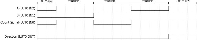
There is a propagation delay from the A and B input signals to the count signal. Consequently, when a quadrature pulse resulting in a changed count signal is received, the change will arrive at LUT0 IN0 after the corresponding change on LUT0 IN1 or IN2. If the LUT output is not filtered, it will cause a glitch on LUT0 OUT, which will invoke the direction update interrupt unnecessarily. The filter in LUT0 is enabled to mitigate the issue.