| Standard Operating Conditions (unless otherwise stated) | |||||||
|---|---|---|---|---|---|---|---|
| Param. No. | Sym. | Characteristic | Min. | Typ. † | Max. | Units | Conditions |
| SP70* |
TSSL2SCH, TSSL2SCL |
SDO to SCK↓ or SCK↑ input | 2.25*TCY | — | — | ns | |
| SP71* | TSCH | SCK output high time | TCY + 20 | — | 0.5 TSCK + 12 | ns | |
| SP72* | TSCL | SCK output low time | TCY + 20 | — | 0.5 TSCK + 12 | ns | |
| SP73* |
TDIV2SCH, TDIV2SCL |
Setup time of SDI data input to SCK edge | 85 | — | — | ns | |
| SP74* |
TSCH2DIL, TSCL2DIL |
Hold time of SDI data input to SCK edge | 0 | — | — | ns | |
| Hold time of SDI data input to final SCK | 0.5 TSCK | ns | CKE = 0,SMP = |
||||
| SP75* | TDOR | SDO data output rise time | — | 10 | 25 | ns | CL = 50 pF |
| SP76* | TDOF | SDO data output fall time | — | 10 | 25 | ns | CL = 50 pF |
| SP78* | TSCR | SCK output rise time | — | 10 | 25 | ns | CL = 50 pF |
| SP79* | TSCF | SCK output fall time | — | 10 | 25 | ns | CL = 50 pF |
| SP80* |
TSCH2DOV, TSCL2DOV |
SDO data output valid after SCK edge | — | — | — | ns | CL = 50 pF |
| SP81* |
TDOV2SCH, TDOV2SCL |
SDO data output valid to first SCK edge | 1 TCY | — | — | ns |
CL = 50 pF CKE = |
| SP82* | TSSL2DOV | SDO data output valid after SS↓ edge | — | — | 50 | ns | CL = 20 pF |
| SP83* |
TSCH2SSH, TSCL2SSH |
SS ↑ after last SCK edge | 1.5 TCY + 40 | — | — | ns | |
|
* These parameters are characterized but not tested. † Data in “Typ” column is at 3.0V, 25°C unless otherwise stated. These parameters are for design guidance only and are not tested. Note:
|
|||||||
Figure 1. SPI Host Mode Timing (CKE =
0, SMP = 0)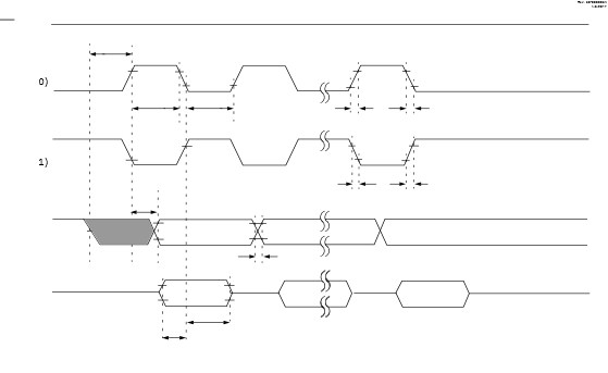
Note: Refer to the “Load
Conditions” figure for load conditions.
Figure 2. SPI Host Mode Timing (CKE =
1, SMP = 1)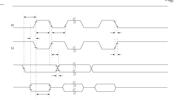
Note: Refer to the “Load
Conditions” figure for load conditions.
Figure 3. SPI Client Mode Timing (CKE =
0)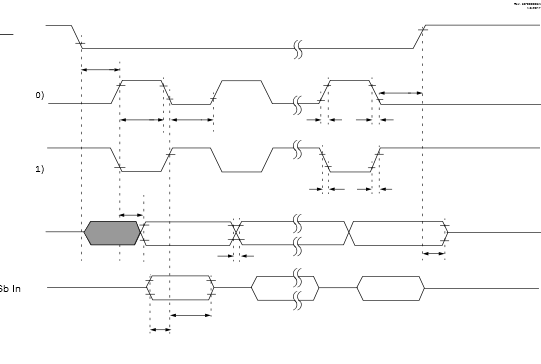
Note: Refer to the “Load
Conditions” figure for load conditions.
Figure 4. SPI Client Mode Timing (CKE =
1)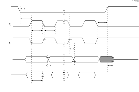
Note: Refer to the “Load
Conditions” figure for load conditions.