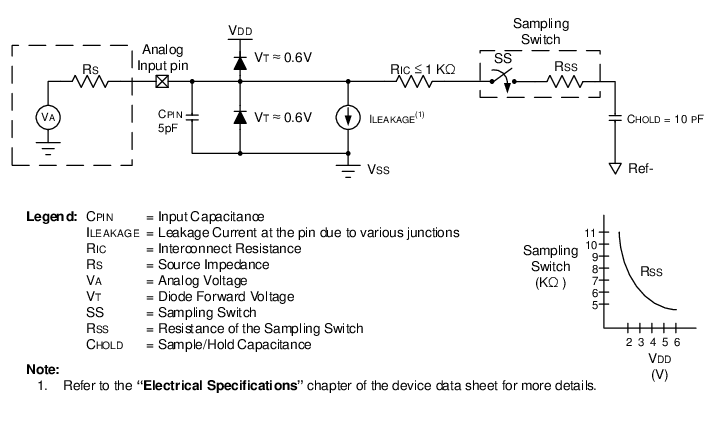
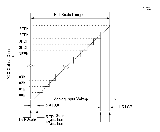
For the ADC to meet its specified accuracy, the charge holding capacitor (CHOLD) must be allowed to fully charge to the input channel voltage level. The analog input model is shown in Figure 2. The source impedance (RS) and the internal sampling switch (RSS) impedance directly affect the time required to charge the capacitor CHOLD. The sampling switch (RSS) impedance varies over the device voltage (VDD). The maximum recommended impedance for analog sources is 10 kΩ. As the source impedance is decreased, the acquisition time may be decreased. After the analog input channel is selected (or changed), an ADC acquisition time must be completed before the conversion can be started. To calculate the minimum acquisition time, Figure 1 may be used. This equation assumes an error of 1/2 LSb. The 1/2 LSb error is the maximum error allowed for the ADC to meet its specified resolution.
Assumptions: Temperature = 50°C; External impedance = 10 kΩ; VDD = 5.0V
TACQ = Amplifier Settling Time + Hold Capacitor Charging Time + Temperature Coefficient
The value for TC can be approximated with the following equations:
Note: Where n = ADC resolution in bits
Solving for TC:
Therefore:
- The reference voltage (VREF) has no effect on the equation, since it cancels itself out
- The charge holding capacitor (CHOLD) is not discharged after each conversion
- The maximum recommended impedance for analog sources is 10 kΩ. This is required to meet the pin leakage specification.