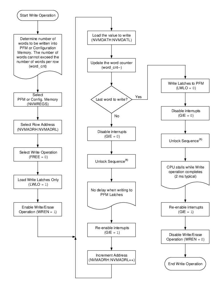
- 1.Load the address of the row to be programmed into NVMADRH:NVMADRL.
- 2.Load each write latch with data via the NMVDATH:NVMDATL registers.
- 3.Initiate a programming operation.
- 4.Repeat steps 1 through 3 until all data is written.
Before writing to program memory, the word(s) to be written must be erased or previously unwritten. Program memory can only be erased one row at a time. No automatic erase occurs upon the initiation of the write.
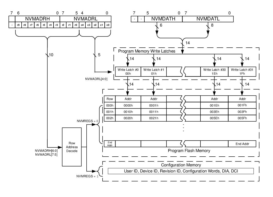
Program memory can be written one or more words at a time. The maximum number of words written at one time is equal to the number of write latches. See Figure 1 for more details.
The write latches are aligned to the Flash row address boundary defined by the upper ten bits of NVMADRH:NVMADRL, (NVMADRH[6:0]:NVMADRL[7:5]) with the lower five bits of NVMADRL, (NVMADRL[4:0]) determining the write latch being loaded. Write operations do not cross these boundaries. At the completion of a program memory write operation, the data in the write latches is reset to contain 0x3FFF.
1. When the last word to be loaded into the write
latch is ready, the LWLO bit is cleared and the unlock sequence executed. This initiates
the programming operation, writing all the latches into Flash program memory.- 1.Set the WREN bit.
- 2.Clear the NVMREGS bit.
- 3.Set the LWLO bit. When the LWLO bit is set (LWLO =
1), the write sequence will only load the write latches and will not initiate the write to Program Flash Memory. - 4.Load the NVMADRH:NVMADRL register pair with the address of the location to be written.
- 5.Load the NVMDATH:NVMDATL register pair with the program memory data to be written.
- 6.Execute the unlock sequence. The write latch is now loaded.
- 7.Increment the NVMADRH:NVMADRL register pair to point to the next location.
- 8.Repeat steps 5 through 7 until all except the last write latch has been loaded.
- 9.Clear the LWLO bit. When the LWLO
bit is clear (LWLO =
0), the write sequence will initiate the write to Program Flash Memory. - 10.Load the NVMDATH:NVMDATL register pair with the program memory data to be written.
- 11.Execute the unlock sequence. The entire program memory latch content is now written to Flash program memory.
An example of the complete write sequence is shown in Writing to Program Flash Memory. The initial address is loaded into the NVMADRH:NVMADRL register pair; the data is loaded using indirect addressing.
Writing to Program Flash Memory
INTCONbits.GIE = 0; // Disable interrupts
// PFM row must be erased before writes can occur
NVMCON1bits.NVMREGS = 0; // Point to PFM
NVMADR = PFMStartAddress; // Must start at beginning of PFM row
NVMCON1bits.FREE = 1; // Specify an erase operation
NVMCON1bits.WREN = 1; // Allow erase cycle
// Required unlock sequence
NVMCON2 = 0x55;
NVMCON2 = 0xAA;
NVMCON1bits.WR = 1;
NVMCON1bits.LWLO = 1; // Load write latches
// Write to the data latches
for (i = 0; i < PFM_ROW_SIZE; i++)
{
NVMADR = PFMStartAddress; // Load starting address
NVMDAT = PFM_WRITE_DATA; // Load data
// Required unlock sequence
NVMCON2 = 0x55;
NVMCON2 = 0xAA;
NVMCON1bits.WR = 1;
PFMStartAddress++; // Increment address
if(i = (PFM_ROW_SIZE - 1)) // All latches loaded?
{
NVMCON1bits.LWLO = 0; // Start PFM write
}
}
NVMCON1bits.WREN = 0; // Disable writes
INTCONbits.GIE = 1; // Enable interrupts