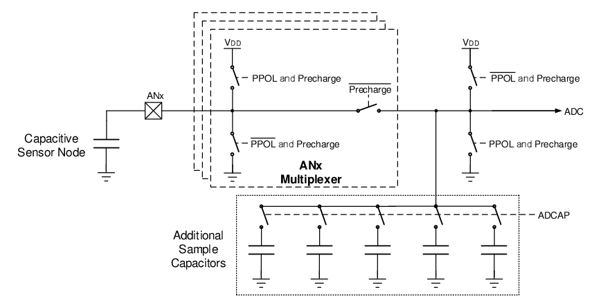
The ADC module contains several features that allow the user to perform a relative capacitance measurement on any ADC channel using the internal ADC Sample-and-Hold capacitance as a reference. This relative capacitance measurement can be used to implement capacitive touch or proximity sensing applications. The following figure shows the basic block diagram of the CVD portion of the ADC module.
Figure 1. Hardware
Capacitive Voltage Divider Block Diagram
This is an example to configure ADC for CVD operation:
- 1.Configure Port:
- a.Disable pin output driver (refer to the TRISx register)
- b.Configure pin as analog (refer to the ANSELx register)
- 2.Configure the ADC module:
- 3.Configure ADC interrupt
(optional):
- a.Clear ADC interrupt flag
- b.Enable ADC interrupt
- c.Enable global interrupt (GIE bit)(1)
- 4.Start double sample conversion by setting the GO bit.
- 5.Wait for ADC conversion to complete
by one of the following:
- Polling the GO bit
- Waiting for the ADC interrupt (if interrupt is enabled)
- 6.Second ADC conversion depends on
the state of CONT:
- a.If CONT =
1, both conversion will repeat automatically form a single trigger. - b.If CONT =
0, each conversion must be triggered separately.
- a.If CONT =
- 7.The ADERR register contains the CVD result.
- 8.Clear the ADC interrupt flag (if interrupt is enabled).
Note:
- 1.With global interrupts disabled (GIE
=
0), the device will wake from Sleep, but will not enter an Interrupt Service Routine.