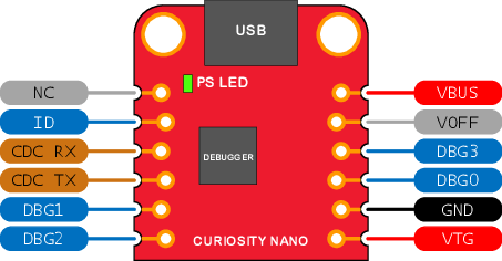
The figure and table below show where the programming and debugging signals must be connected to program and debug external microcontrollers. The on-board debugger can supply power to the external hardware or use an external voltage as a reference for its level shifters. Read more about the power supply in Power Supply.
The on-board debugger and level shifters actively drive data and clock signals used for programming and debugging (DBG0, DBG1, and DBG2). Usually, the external resistor on these signals can be ignored. Pull-down resistors are required on the ICSP™ data and clock signals to debug PIC® microcontrollers.
DBG3 is an open-drain connection and requires a pull-up resistor to function.
- Connect GND and VTG to the external microcontroller
- Tie the VOFF pin to GND if the external hardware has a power supply
- Make sure there are pull-down resistors on the ICSP data and clock signals (DBG0 and DBG1) to support the debugging of PIC microcontrollers
| Curiosity Nano Pin | UPDI | ICSP™ | SWD |
|---|---|---|---|
| DBG0 | UPDI | DATA | SWDIO |
| DBG1 | — | CLK | SWCLK |
| DBG2 | — | — | — |
| DBG3 | — | MCLR | RESET |