The potential scenarios where the periodic noise occurs are switch mode regulators or PWM signals used for motor or LED control, etc.
With the feature hardware sample accumulator, average value of the accumulated samples can be calculated by dividing the accumulated result by burst size (number of samples accumulated) and resulting in a zero mean sampled noise.
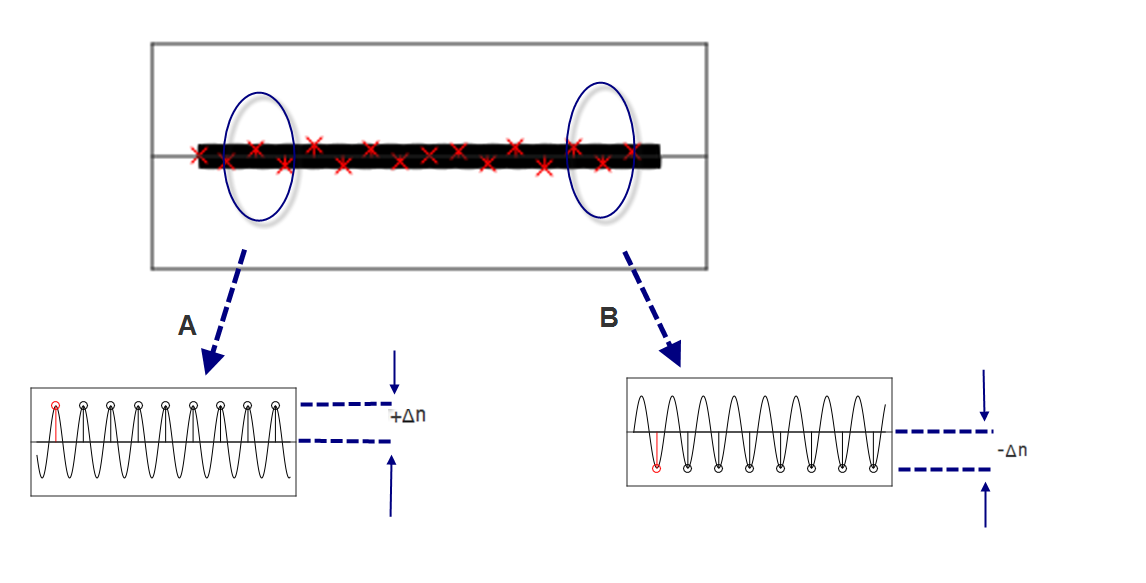
Consider a DC signal mixed with periodic noise and an accumulation of multiple samples shown with red markings, as in Figure 1.
If the signal is zoomed, consider ADC samples which are taken in part 'A' and part 'B' in Figure 1.
As a hardware sample accumulator is used, the average result of ADC samples in part 'A' will be ≅ +Δn. In part 'B', the average result of ADC samples will be ≅ -Δn. As each individual sample differ from zero with equal probability of being either positive or negative, the accumulated noise samples will approach zero, and the noise is successfully suppressed.
Sampling Delay or Automatic Sampling Delay Variation:
When the periodic noise frequency is known, the sampling rate can be adjusted to tune the sampling frequency away from any periodic or harmonic noise aliased with the ADC sampling frequency (within the burst) from the sampled signal.
In case of unknown periodic noise frequency, an automatic sampling delay variation feature can be used to randomize this delay to slightly change the time between samples and achieve better noise suppression. In this case, broader suppression range is achieved but with reduced noise attenuation.
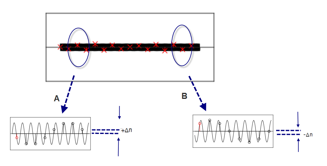
If sampling delay is added and sampling frequency is adjusted, consider that the actual read ADC samples are as shown in part 'A' and 'B' in Figure 2. In this scenario, the average value of samples taken in batch 'A' will be close to zero and the average value of the samples taken in batch 'B' will be equally close to zero, and it results in suppressing the noise signal.
The sampling delay and sampling length can be adjusted using the Sample Delay bit field in the Control D (ADC.CTRLD) register and the Sample Length bit field in the Sample Control (ADC.SAMPCTRL) register. Both of these control the ADC sampling time in CLK_ADC cycles.
Total sampling time is given by:
In Free-Running mode, the sampling rate RS is calculated by:
Sampling Delay Selection bits in the ADC.CTRLD register define the delay between consecutive ADC samples. The SAMPDLY field can also be automatically modified from one sampling cycle to another, by setting the ASDV bit. The delay is expressed as CLK_ADC cycles. When the ASDV bit is not enabled, the SAMPDLY value can be configured from 0 to 15. 0 means no sampling delay, 1 is a delay of 1 cycle, and so on. In the setup, it is required to tune this value correctly for obtaining the desired results and to suppress the present frequency components. It is needed to configure this value by a trial-and-error method so that +Δn or -Δn is close to zero.
From the above figures it can be seen that with a correctly tuned value of the sampling delay (SMPDLY) between consecutive samples, the average result of ADC samples approach the noise free signal.
With an increase in sampling delay or number of samples accumulated, the sampling frequency is reduced.