Each LUT pair can be connected to internal sequential logic: D flip flop, JK flip flop, gated D-latch or RS-latch can be selected by writing the corresponding Sequential Selection bits in Sequential Control x register (SEQCTRLx.SEQSEL). Before using sequential logic, the GCLK clock and optionally each LUT filter or edge detector, must be enabled.
Gated D Flip-Flop (DFF)
When the DFF is selected, the D-input is driven by the even LUT output (LUT2x), and the G-input is driven by the odd LUT output (LUT2x+1), as shown in Figure 1.
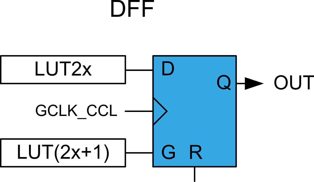
When the even LUT is disabled (LUTCTRL2x.ENABLE=0), the flip-flop is asynchronously cleared. The reset command (R) is kept enabled for one APB clock cycle. In all other cases, the flip-flop output (OUT) is refreshed on rising edge of the GCLK_CCL, as shown in Table 1.
| R | G | D | OUT |
|---|---|---|---|
| 1 | X | X | Clear |
| 0 | 1 | 1 | Set |
| 0 | Clear | ||
| 0 | X | Hold state (no change) |
JK Flip-Flop (JK)
When this configuration is selected, the J-input is driven by the even LUT output (LUT2x), and the K-input is driven by the odd LUT output (LUT2x+1), as shown in Figure 2.
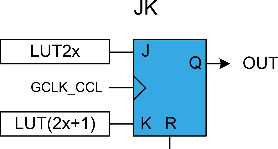
When the even LUT is disabled (LUTCTRL2x.ENABLE=0), the flip-flop is asynchronously cleared. The reset command (R) is kept enabled for one APB clock cycle. In all other cases, the flip-flop output (OUT) is refreshed on rising edge of the GCLK_CCL, as shown in Table 2.
| R | J | K | OUT |
|---|---|---|---|
| 1 | X | X | Clear |
| 0 | 0 | 0 | Hold state (no change) |
| 0 | 0 | 1 | Clear |
| 0 | 1 | 0 | Set |
| 0 | 1 | 1 | Toggle |
Gated D-Latch (DLATCH)
When the DLATCH is selected, the D-input is driven by the even LUT output (LUT2x), and the G-input is driven by the odd LUT output (LUT2x+1), as shown in Figure 1.
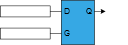
When the even LUT is disabled (LUTCTRL2x.ENABLE=0), the latch output will be cleared. The G-input is forced enabled for one more APB clock cycle, and the D-input to zero. In all other cases, the latch output (OUT) is refreshed as shown in Table 3.
| G | D | OUT |
|---|---|---|
| 0 | X | Hold state (no change) |
| 1 | 0 | Clear |
| 1 | 1 | Set |
RS Latch (RS)
When this configuration is selected, the S-input is driven by the even LUT output (LUT2x), and the R-input is driven by the odd LUT output (LUT2x+1), as shown in Figure 4.
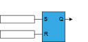
When the even LUT is disabled (LUTCTRL2x.ENABLE=0), the latch output will be cleared. The R-input is forced enabled for one more APB clock cycle and S-input to zero. In all other cases, the latch output (OUT) is refreshed as shown in Table 4.
| S | R | OUT |
|---|---|---|
| 0 | 0 | Hold state (no change) |
| 0 | 1 | Clear |
| 1 | 0 | Set |
| 1 | 1 | Forbidden state |