The application may need to detect when a specific combination of signals (pattern) appears on the pins. By combining logic gates, a simple state decoder for external signals can be implemented without involving the CPU.
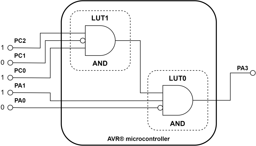
In this example, the CCL module will be used to decode the presence of the
b’10110 pattern on the input pins. LUT0 and LUT1, connected to the
corresponding input pins, will be used.
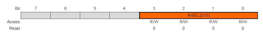
The input selection from different input options is done using the INSELx[3:0] bits from the LUT Control (LUTnCTRLB and LUTnCTRLC) registers, as shown in the following figures.

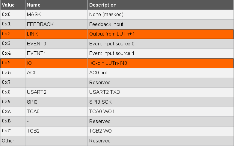
The table below summarizes the INSEL[3:0] options for all inputs.
For this example, two adjacent LUTs (LUT0 and LUT1) will be used, with the output of LUT1 connected to the LUT0 input (linked).
CCL.LUT0CTRLC = CCL_INSEL2_LINK_gc;
The other two inputs of LUT0 and all three inputs of LUT1 are connected to the I/O pins.
CCL.LUT0CTRLB = CCL_INSEL0_IO_gc | CCL_INSEL1_IO_gc;
CCL.LUT1CTRLB = CCL_INSEL0_IO_gc | CCL_INSEL1_IO_gc;

CCL.LUT1CTRLC = CCL_INSEL2_IO_gc;
The following step is to configure the truth tables for LUT0 and LUT1 to generate the
right combinational logic to detect b’10110 on the selected pins. The
TRUTH1 table is used to decode the pattern for the Most Significant three bits
(b’10110).
CCL.TRUTH1 = 0x20;
LUT0 has as inputs two Least Significant bits from the input pattern
(b’10110) and the decoded output of LUT1 on the third input,
resulting in binary sequence b’110 to be decoded. The value of the
truth table, in this case, will be 0x40.
CCL.TRUTH0 = 0x40;
The next step is to configure the output of the decoder, specifically, the I/O PORT pin PA3 in this example. This is done by setting the OUTEN bit on the LUT0CTRLA register.

This translates to the following code.
CCL.LUT0CTRLA = CCL_OUTEN_bm;
By enabling the LUTn output on the I/O pin, the settings for the corresponding pin are overwritten. To complete the setup and the start decoding of the input sequence, the CCL and used LUTs need to be enabled. That is done using the ENABLE bit from the LUTnCTRLA register.
CCL.LUT1CTRLA = CCL_ENABLE_bm;
CCL.LUT0CTRLA |= CCL_ENABLE_bm;
To complete the setup, the CCL module needs to be enabled using a CCL Global Enable bit from the CTRLA register.

CCL.CTRLA = CCL_ENABLE_bm;

An MCC generated code example for AVR128DA48, with the same functionality as the one described in this section, can be found here: